Microelectronic Engineering ( IF 2.3 ) Pub Date : 2024-01-03 , DOI: 10.1016/j.mee.2024.112132 Zijing Xie , Nianhe Xiong , Jun Tang , Hong Wang
|
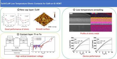
We proposed a low temperature Au-free ohmic contacts of GaN-on-Si HEMT with the Ta/Al/CuW metal stack. The CuW was deposited by using the dual-target magnetron sputter deposition method. The annealing conditions and recess depth of ohmic area were systematically investigated. By utilizing the Ta/Al/CuW structure, an improved contact characteristic (0.49 Ω·mm) is obtained following annealing at 550 °C for 10 min in vacuum, with the recess depth of 30 nm(±2 nm). This performance surpasses that of Ta/Al/W Au-free contacts (1.07 Ω·mm). Furthermore, both the Ta/Al/CuW ohmic contacts (RMS = 6.3 nm) and the Ta/Al/W ohmic contacts (RMS = 6.0 nm) exhibit smooth surface morphology. Compared to Ti contact layer, Ta demonstrates superior performance in low temperature contact and breakdown test. Amorphous Ta layer can effectively suppress Cu diffusion. The GaN-on-Si HEMT was also fabricated based on Ta/Al/CuW Au-free ohmic contacts, exhibiting excellent DC characteristics.
中文翻译:
用于 GaN-on-Si HEMT 的 Ta/Al/CuW 低温欧姆接触
我们提出了GaN-on-Si HEMT 与 Ta/Al/CuW 金属堆叠的低温无金欧姆接触。采用双靶磁控溅射沉积方法沉积CuW 。对退火条件和欧姆区凹陷深度进行了系统研究。利用Ta/Al/CuW结构,在真空中550℃退火10分钟后,获得了改善的接触特性(0.49Ω·mm),凹陷深度为30nm(±2nm)。该性能超过了 Ta/Al/W 无 Au 触点 (1.07 Ω·mm)。此外,Ta/Al/CuW 欧姆接触(RMS = 6.3 nm)和 Ta/Al/W 欧姆接触(RMS = 6.0 nm)均表现出光滑的表面形貌。与Ti接触层相比,Ta在低温接触和击穿测试中表现出优越的性能。非晶Ta层可以有效抑制Cu扩散。GaN-on-Si HEMT 也是基于 Ta/Al/CuW 无金欧姆接触制造的,表现出优异的直流特性。


 京公网安备 11010802027423号