Nature Nanotechnology ( IF 38.3 ) Pub Date : 2024-01-16 , DOI: 10.1038/s41565-023-01581-2 Hyeon-Dong Lee , Seung-Je Woo , Sungjin Kim , Junho Kim , Huanyu Zhou , Shin Jung Han , Kyung Yeon Jang , Dong-Hyeok Kim , Jinwoo Park , Seunghyup Yoo , Tae-Woo Lee
|
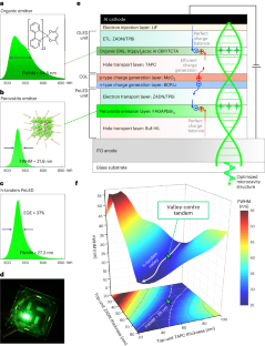
Perovskite light-emitting diodes (PeLEDs) have emerged as a promising new light source for displays. The development roadmap for commercializing PeLEDs should include a tandem device structure, specifically by stacking a thin nanocrystal PeLED unit and an organic light-emitting diode unit, which can achieve a vivid and efficient tandem display; however, simply combining light-emitting diodes with different characteristics does not guarantee both narrowband emission and high efficiency, as it may cause a broadened electroluminescence spectra and a charge imbalance. Here, by conducting optical simulations of the hybrid tandem (h-tandem) PeLED, we have discovered a crucial optical microcavity structure known as the h-tandem valley, which enables the h-tandem PeLED to emit light with a narrow bandwidth. Specifically, the centre structure of the h-tandem valley (we call it valley-centre tandem) demonstrates near-perfect charge balance and optimal microcavity effects. As a result, the h-tandem PeLED achieves a high external quantum efficiency of 37.0% and high colour purity with a narrow full-width at half-maximum of 27.3 nm (versus 64.5 nm in organic light-emitting diodes) along with a fast on–off response. These findings offer a new strategy to overcome the limitations of nanocrystal-based PeLEDs, providing valuable optical and electrical guidelines for integrating different types of light-emitting device into practical display applications.
中文翻译:
谷心串联钙钛矿发光二极管
钙钛矿发光二极管(PeLED)已成为一种有前途的新型显示器光源。PeLED商业化的发展路线应包括串联器件结构,具体是通过堆叠薄的纳米晶PeLED单元和有机发光二极管单元,可以实现生动且高效的串联显示;然而,简单地组合具有不同特性的发光二极管并不能保证窄带发射和高效率,因为它可能导致电致发光光谱变宽和电荷不平衡。在这里,通过对混合串联(h-tandem)PeLED进行光学模拟,我们发现了一种关键的光学微腔结构,称为h-tandem谷,它使h-tandem PeLED能够发射窄带宽的光。具体来说,h 串联谷的中心结构(我们称之为谷中心串联)表现出近乎完美的电荷平衡和最佳的微腔效应。因此,h 串联 PeLED 实现了 37.0% 的高外量子效率和高色纯度,窄半峰全宽为 27.3 nm(有机发光二极管为 64.5 nm),并且具有快速开-关响应。这些发现提供了一种克服基于纳米晶体的 PeLED 局限性的新策略,为将不同类型的发光器件集成到实际显示应用中提供了有价值的光学和电学指南。


 京公网安备 11010802027423号