Journal of Applied Mechanics and Technical Physics ( IF 0.6 ) Pub Date : 2024-01-15 , DOI: 10.1134/s0021894423050061 E. A. Baranov , V. A. Nepomnyashchikh , V. O. Konstantinov , V. G. Shchukin , I. E. Merkulova , A. O. Zamchiy , N. A. Lunev , V. A. Volodin , A. A. Shapovalova
|
Abstract
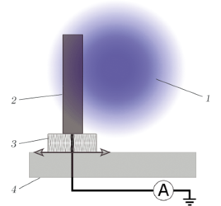
Electron-beam annealing of an amorphous silicon suboxide thin film with a stoichiometric coefficient of 0.5 was carried out in a vacuum chamber. The exposure time was 10 min at an accelerating electron-beam voltage of 1000 V and a current strength of 75 mA. Using probe measurements and calculations, the current density distribution over the electron-beam cross section was obtained assuming a normal distribution. The current density on the beam axis was 0.8 mA/mm2. The electron-beam annealing of the amorphous silicon suboxide thin film led to the formation of crystalline silicon nanoparticles with a size of \((4.1\pm 0.1)\) nm. The crystallite sizes did not depend on the electron-beam current density, in contrast to the degree of crystallinity, which decreased from 40% on the beam axis to zero (amorphous structure) on the periphery. It is suggested that during the formation of nanocrystalline silicon, a liquid phase is formed.
中文翻译:
电子束退火下电流密度对非晶低氧化硅薄膜结构的影响
摘要
在真空室中对化学计量系数为0.5的非晶低氧化硅薄膜进行电子束退火。曝光时间为10分钟,加速电子束电压为1000V,电流强度为75mA。使用探针测量和计算,假设呈正态分布,获得电子束横截面上的电流密度分布。射束轴上的电流密度为0.8mA/mm 2。非晶低氧化硅薄膜的电子束退火导致形成尺寸为 \((4.1\pm 0.1)\) nm的晶体硅纳米颗粒。与结晶度相反,微晶尺寸不依赖于电子束电流密度,结晶度从束轴上的 40% 降低到外围的零(非晶结构)。这表明在纳米晶硅的形成过程中,形成了液相。


 京公网安备 11010802027423号