Analog Integrated Circuits and Signal Processing ( IF 1.4 ) Pub Date : 2024-01-31 , DOI: 10.1007/s10470-023-02243-y Yuping Li , Haihua Wang , Mohammad Trik
|
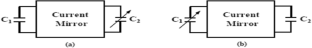
Analog and digital integrated circuit performance has greatly benefited by the shrinking of semiconductor fabrication technology components. In order to reduce the size of the transistors, it is obvious that the speed of the circuits must increase and the supply voltage must decrease. Although this decreases the power consumption of the circuits, it typically reduces the characteristics of analog circuits, such as dynamic range and output resistance. The gift In this study, a novel wide bandwidth current mirror with low power consumption, low voltage, and super high voltage swing are given. The proposed design calls for a current mirror bandwidth of 168 MHz. Additionally, the output impedance for the proposed circuit, which is exceptionally high and is close to 175 MΩ according to the simulation results, guarantees the high accuracy of the suggested current mirror current. The suggested circuit design's low power consumption of 42.4 μW, lowest output voltage of 100 mV, and maximum swing limit of 850 mV all demonstrate that they are ideally suited for low power/operational voltage applications and ultra-low voltage circuit design. And resists less-than-ideal PVT circumstances. The capability of this technique to achieve high-speed current mirror and high-current driving capabilities with few accuracy or power performance restrictions is demonstrated in this work. It is implemented in 0.18 m AMS CMOS technology with a 1 V supply voltage and offers a high output current with a relative current copy error of 2% and a maximum settling time of 2–4 ns, making it well suited for the implementation of quick and balanced multipole current sources.
中文翻译:
一种新型低功耗高性能输出阻抗电流镜电路的设计与仿真
模拟和数字集成电路的性能大大受益于半导体制造技术元件的缩小。为了减小晶体管的尺寸,显然必须提高电路的速度并且必须降低电源电压。虽然这降低了电路的功耗,但它通常会降低模拟电路的特性,例如动态范围和输出电阻。礼物在这项研究中,给出了一种新型的低功耗、低电压和超高电压摆幅的宽带宽电流镜。所提出的设计要求电流镜带宽为 168 MHz。此外,根据仿真结果,所提出电路的输出阻抗非常高,接近 175 MΩ,保证了建议电流镜电流的高精度。建议的电路设计具有 42.4 μW 的低功耗、100 mV 的最低输出电压和 850 mV 的最大摆幅限制,这些都表明它们非常适合低功耗/工作电压应用和超低压电路设计。并能抵抗不太理想的 PVT 情况。这项工作证明了该技术能够在精度或功率性能限制很少的情况下实现高速电流镜和高电流驱动能力。它采用 0.18 m AMS CMOS 技术实现,电源电压为 1 V,提供高输出电流,相对电流复制误差为 2%,最大稳定时间为 2–4 ns,非常适合实现快速和平衡多极电流源。


 京公网安备 11010802027423号