Microsystems & Nanoengineering ( IF 7.9 ) Pub Date : 2024-02-23 , DOI: 10.1038/s41378-024-00655-y Berke Erbas , Ana Conde-Rubio , Xia Liu , Joffrey Pernollet , Zhenyu Wang , Arnaud Bertsch , Marcos Penedo , Georg Fantner , Mitali Banerjee , Andras Kis , Giovanni Boero , Juergen Brugger
|
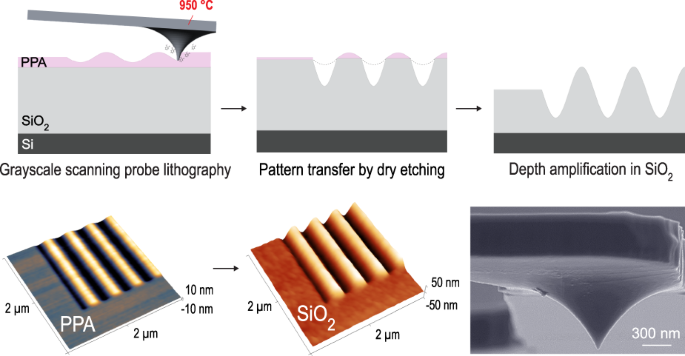
Grayscale structured surfaces with nanometer-scale features are used in a growing number of applications in optics and fluidics. Thermal scanning probe lithography achieves a lateral resolution below 10 nm and a vertical resolution below 1 nm, but its maximum depth in polymers is limited. Here, we present an innovative combination of nanowriting in thermal resist and plasma dry etching with substrate cooling, which achieves up to 10-fold amplification of polymer nanopatterns into SiO2 without proportionally increasing surface roughness. Sinusoidal nanopatterns in SiO2 with 400 nm pitch and 150 nm depth are fabricated free of shape distortion after dry etching. To exemplify the possible applications of the proposed method, grayscale dielectric nanostructures are used for scalable manufacturing through nanoimprint lithography and for strain nanoengineering of 2D materials. Such a method for aspect ratio amplification and smooth grayscale nanopatterning has the potential to find application in the fabrication of photonic and nanoelectronic devices.
中文翻译:
结合热扫描探针光刻和干法蚀刻进行灰度纳米图案放大
具有纳米级特征的灰度结构化表面在光学和流体学领域的应用越来越多。热扫描探针光刻实现了10 nm以下的横向分辨率和1 nm以下的垂直分辨率,但其在聚合物中的最大深度有限。在此,我们提出了热阻纳米写入和等离子干法蚀刻与基板冷却的创新组合,可将聚合物纳米图案放大 10 倍到 SiO 2中,而无需按比例增加表面粗糙度。SiO 2中的正弦纳米图案具有400 nm节距和150 nm深度,在干法蚀刻后没有形状变形。为了举例说明所提出的方法的可能应用,灰度介电纳米结构用于通过纳米压印光刻进行可扩展制造以及二维材料的应变纳米工程。这种纵横比放大和平滑灰度纳米图案化的方法有可能在光子和纳米电子器件的制造中得到应用。


 京公网安备 11010802027423号