Semiconductors ( IF 0.7 ) Pub Date : 2024-03-13 , DOI: 10.1134/s1063782623050159 S. O. Slipchenko , O. S. Soboleva , A. A. Podoskin , Y. K. Kirichenko , T. A. Bagaev , I. V. Yarotskaya , N. A. Pikhtin
|
Abstract
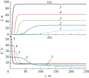
A series of heterostructure designs of low-voltage InP homothyristors have been investigated using numerical simulation methods. The design with a space charge layer formed in the p-base region of the n‒p‒n transistor part was considered as the base one. The dynamic characteristics and processes that determine the rate of transition to the on state are investigated. It is shown that as the p-base thickness increases from 1 to 2.6 μm, the maximum on-state currents increase from 70 to 90 A, while the minimum turn-on transition time is 11 ns at a maximum blocking voltage of 55 V. It is shown that the operation efficiency in the on state is determined by the residual voltage. Residual voltage decreases with a decrease in the thickness of the p-base.
中文翻译:
低压 InP 同晶闸管的开关(导通)动态
摘要
使用数值模拟方法研究了一系列低压 InP 同质晶闸管的异质结构设计。在n - p - n晶体管部分的p基极区域形成空间电荷层的设计被认为是基础设计。研究了决定转换到导通状态的速率的动态特性和过程。结果表明,随着p基极厚度从 1 μm 增加到 2.6 μm,最大通态电流从 70 A 增加到 90 A,而在最大阻断电压 55 V 时,最小导通过渡时间为 11 ns。结果表明,导通状态下的工作效率由残余电压决定。残余电压随着p基极厚度的减小而减小。


 京公网安备 11010802027423号