Semiconductors ( IF 0.7 ) Pub Date : 2024-03-13 , DOI: 10.1134/s1063782623070138 M. V. Lebedev , T. V. Lvova , A. N. Smirnov , V. Yu. Davydov , A. V. Koroleva , E. V. Zhizhin , S. V. Lebedev
|
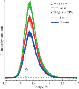
Photoluminescence, Raman spectroscopy and X-ray photoelectron spectroscopy are used to study electronic and atomic structure of n-InP(100) surfaces treated with different sulfide solutions. It is shown that the sulfide treatment causes removal of the native oxide layer from the semiconductor surface and formation of the passivating layer consisting of In–S chemical bonds with the structure dependent on the solution composition and atomic arrangement at the initial surface of the semiconductor. This is accompanied by an increase in photoluminescence intensity and narrowing of the surface depletion layer. Atomic structure of the passivating layer determines the total dipole that modifies the depth distribution of the bands potentials and thus the surface electronic structure.
中文翻译:
钝化 n-InP(100) 表面电子结构和原子结构的相关性
利用光致发光、拉曼光谱和X射线光电子能谱研究经不同硫化物溶液处理的n -InP(100)表面的电子和原子结构。研究表明,硫化物处理会去除半导体表面的原生氧化层,并形成由 In-S 化学键组成的钝化层,其结构取决于半导体初始表面的溶液成分和原子排列。这伴随着光致发光强度的增加和表面耗尽层的变窄。钝化层的原子结构决定了总偶极子,该偶极子改变了能带势的深度分布,从而改变了表面电子结构。


 京公网安备 11010802027423号