当前位置:
X-MOL 学术
›
Adv. Electron. Mater.
›
论文详情
Our official English website, www.x-mol.net, welcomes your feedback! (Note: you will need to create a separate account there.)
Area and Device Count Efficient Binary Logic Circuits using Anti‐Ambipolar Switch Devices
Advanced Electronic Materials ( IF 6.2 ) Pub Date : 2024-03-15 , DOI: 10.1002/aelm.202300892 Jae Hyeon Jun 1 , Yongsu Lee 1 , Hae‐Won Lee 1 , Minjae Kim 1 , Hyeon Jun Hwang 1 , Byoung Hun Lee 1
Advanced Electronic Materials ( IF 6.2 ) Pub Date : 2024-03-15 , DOI: 10.1002/aelm.202300892 Jae Hyeon Jun 1 , Yongsu Lee 1 , Hae‐Won Lee 1 , Minjae Kim 1 , Hyeon Jun Hwang 1 , Byoung Hun Lee 1
Affiliation
|
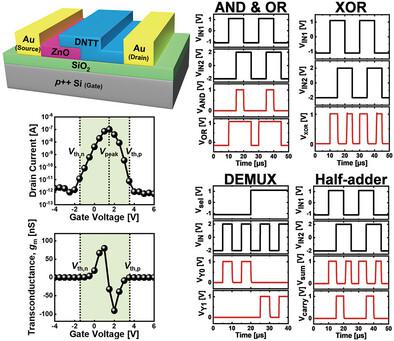
The unique characteristics of an anti‐ambipolar switch (AAS) device exhibit Λ‐shaped transfer responses (namely delta conductance) and present unique opportunities to overcome the limit of silicon‐based, complementary metal‐oxide‐semiconductor (CMOS) logic circuits. It is crucial because a device that only turns on under a certain bias range can be utilized to simplify the logic circuit and reduce the device count and circuit area required to perform logic functions. In this study, a physically scalable AAS device is investigated using ZnO and dinaphtho[2,3‐b :2′,3′‐f ]thieno[3,2‐b ]thiophene as heterojunction structures to reduce the operating voltage and enhance the peak current and peak‐to‐valley ratio of the AAS device. Moreover, novel logic circuits for AND, OR, XOR, DEMUX, and half‐adder functions are demonstrated using AAS devices. AAS device‐based logic circuits exhibit power‐efficiency characteristics (≈49 times lower than that of the 90‐nm silicon‐based CMOS inverter) and reduce the transistor count and the circuit area by ≈67% and ≈70%, respectively. These results indicate that the use of AAS device‐based logic circuits can be a promising approach to overcome the physical scaling limit of current CMOS technology.
中文翻译:

使用抗双极性开关器件的面积和器件数量高效的二进制逻辑电路
反双极开关(AAS)器件的独特特性表现出Λ形转移响应(即电导增量),并为克服硅基互补金属氧化物半导体(CMOS)逻辑电路的限制提供了独特的机会。这是至关重要的,因为可以利用仅在一定偏置范围下导通的器件来简化逻辑电路并减少执行逻辑功能所需的器件数量和电路面积。在本研究中,使用 ZnO 和二萘酚 [2,3-] 研究了一种物理可扩展的 AAS 装置乙 :2′,3′-F ] 噻吩诺[3,2‐乙 ]噻吩作为异质结结构,以降低工作电压并提高AAS器件的峰值电流和峰谷比。此外,还使用 AAS 器件演示了用于 AND、OR、XOR、DEMUX 和半加器功能的新颖逻辑电路。基于 AAS 器件的逻辑电路表现出功率效率特性(比 90 nm 硅基 CMOS 反相器低约 49 倍),并将晶体管数量和电路面积分别减少约 67% 和约 70%。这些结果表明,使用基于 AAS 器件的逻辑电路可能是克服当前 CMOS 技术物理缩放限制的一种有前途的方法。
更新日期:2024-03-15
中文翻译:
使用抗双极性开关器件的面积和器件数量高效的二进制逻辑电路
反双极开关(AAS)器件的独特特性表现出Λ形转移响应(即电导增量),并为克服硅基互补金属氧化物半导体(CMOS)逻辑电路的限制提供了独特的机会。这是至关重要的,因为可以利用仅在一定偏置范围下导通的器件来简化逻辑电路并减少执行逻辑功能所需的器件数量和电路面积。在本研究中,使用 ZnO 和二萘酚 [2,3-] 研究了一种物理可扩展的 AAS 装置


 京公网安备 11010802027423号