当前位置:
X-MOL 学术
›
ACS Photonics
›
论文详情
Our official English website, www.x-mol.net, welcomes your feedback! (Note: you will need to create a separate account there.)
Scalable On-Chip Optoelectronic Ising Machine Utilizing Thin-Film Lithium Niobate Photonics
ACS Photonics ( IF 7 ) Pub Date : 2024-03-14 , DOI: 10.1021/acsphotonics.4c00003 Zhenhua Li 1 , Ranfeng Gan 1 , Zihao Chen 1 , Zhaoang Deng 1 , Ran Gao 2 , Kaixuan Chen 3 , Changjian Guo 3 , Yanfeng Zhang 1, 4 , Liu Liu 5, 6 , Siyuan Yu 1 , Jie Liu 1
ACS Photonics ( IF 7 ) Pub Date : 2024-03-14 , DOI: 10.1021/acsphotonics.4c00003 Zhenhua Li 1 , Ranfeng Gan 1 , Zihao Chen 1 , Zhaoang Deng 1 , Ran Gao 2 , Kaixuan Chen 3 , Changjian Guo 3 , Yanfeng Zhang 1, 4 , Liu Liu 5, 6 , Siyuan Yu 1 , Jie Liu 1
Affiliation
|
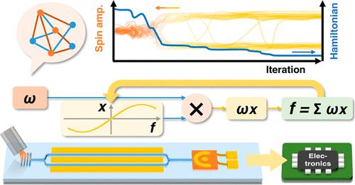
The Ising machine (IM) has emerged as a promising tool for tackling nondeterministic polynomial-time hard combinatorial optimization problems in real-world applications. Among various types of IMs, optoelectronic IMs based on electro-optical (EO) modulators stand out as an impressive platform for Ising computations. They offer a simple and stable architecture, with the EO modulator providing a natural inline nonlinear transfer function for the Ising model. However, integrated optoelectronic IMs have not been demonstrated until now, and exploring large-scale computations within the constraints of digital hardware resources remains an open challenge for these systems. In this paper, an integrated optoelectronic IM based on a thin-film lithium niobate (TFLN) photonic chip is presented, in conjunction with a sparse matrix–vector multiplication algorithm embedded in a field-programmable gate array that optimizes hardware resource utilization and minimizes computational latency. This setup allows us to solve multiple types of MAX-CUT problems with up to 2048 spins and achieve a remarkably low iteration latency of 1.78 μs. To further address the constraints posed by digital devices when tackling larger-scale Ising problems, we extend the application of the TFLN chip to yet another new scheme in which the single, compact on-chip modulator concurrently performs operations of linear multiplication and nonlinear transformation. This scheme demonstrates the capability to address large-scale MAX-CUT problems involving up to 16,384 spins, which, to the best of our knowledge, are the largest-scale problems solved on an on-chip IM, highlighting its potential to overcome digital limitations. The TFLN-based optoelectronic IMs provide a compact solution with high scalability for potentially practical applications in addressing complex combinatorial optimization problems.
中文翻译:

利用薄膜铌酸锂光子学的可扩展片上光电 Ising 机
伊辛机 (IM) 已成为解决现实应用中的非确定性多项式时间硬组合优化问题的有前途的工具。在各种类型的 IM 中,基于电光 (EO) 调制器的光电 IM 脱颖而出,成为令人印象深刻的伊辛计算平台。它们提供简单而稳定的架构,EO 调制器为 Ising 模型提供自然的内联非线性传递函数。然而,集成光电 IM 至今尚未得到证实,在数字硬件资源的限制下探索大规模计算仍然是这些系统面临的一个开放挑战。本文提出了一种基于薄膜铌酸锂(TFLN)光子芯片的集成光电 IM,结合嵌入现场可编程门阵列的稀疏矩阵向量乘法算法,可优化硬件资源利用率并最大限度地减少计算量。潜伏。此设置使我们能够解决最多 2048 个旋转的多种类型的 MAX-CUT 问题,并实现 1.78 μs 的极低迭代延迟。为了进一步解决数字设备在处理更大规模 Ising 问题时所带来的限制,我们将 TFLN 芯片的应用扩展到另一种新方案,其中单个紧凑的片上调制器同时执行线性乘法和非线性变换操作。该方案展示了解决涉及多达 16,384 次旋转的大规模 MAX-CUT 问题的能力,据我们所知,这是在片上 IM 上解决的最大规模问题,凸显了其克服数字限制的潜力。基于 TFLN 的光电 IM 为解决复杂组合优化问题的潜在实际应用提供了具有高可扩展性的紧凑解决方案。
更新日期:2024-03-14
中文翻译:
利用薄膜铌酸锂光子学的可扩展片上光电 Ising 机
伊辛机 (IM) 已成为解决现实应用中的非确定性多项式时间硬组合优化问题的有前途的工具。在各种类型的 IM 中,基于电光 (EO) 调制器的光电 IM 脱颖而出,成为令人印象深刻的伊辛计算平台。它们提供简单而稳定的架构,EO 调制器为 Ising 模型提供自然的内联非线性传递函数。然而,集成光电 IM 至今尚未得到证实,在数字硬件资源的限制下探索大规模计算仍然是这些系统面临的一个开放挑战。本文提出了一种基于薄膜铌酸锂(TFLN)光子芯片的集成光电 IM,结合嵌入现场可编程门阵列的稀疏矩阵向量乘法算法,可优化硬件资源利用率并最大限度地减少计算量。潜伏。此设置使我们能够解决最多 2048 个旋转的多种类型的 MAX-CUT 问题,并实现 1.78 μs 的极低迭代延迟。为了进一步解决数字设备在处理更大规模 Ising 问题时所带来的限制,我们将 TFLN 芯片的应用扩展到另一种新方案,其中单个紧凑的片上调制器同时执行线性乘法和非线性变换操作。该方案展示了解决涉及多达 16,384 次旋转的大规模 MAX-CUT 问题的能力,据我们所知,这是在片上 IM 上解决的最大规模问题,凸显了其克服数字限制的潜力。基于 TFLN 的光电 IM 为解决复杂组合优化问题的潜在实际应用提供了具有高可扩展性的紧凑解决方案。


 京公网安备 11010802027423号