当前位置:
X-MOL 学术
›
Phys. Status Solidi B
›
论文详情
Our official English website, www.x-mol.net, welcomes your feedback! (Note: you will need to create a separate account there.)
Origin of Black Color in Heavily Doped n‐Type GaN Crystal
Physica Status Solidi (B) - Basic Solid State Physics ( IF 1.6 ) Pub Date : 2024-03-16 , DOI: 10.1002/pssb.202400027 Tomoaki Sumi 1 , Junichi Takino 1 , Yoshio Okayama 1 , Shigeyoshi Usami 2 , Masayuki Imanishi 2 , Masashi Yoshimura 2 , Yusuke Mori 2
Physica Status Solidi (B) - Basic Solid State Physics ( IF 1.6 ) Pub Date : 2024-03-16 , DOI: 10.1002/pssb.202400027 Tomoaki Sumi 1 , Junichi Takino 1 , Yoshio Okayama 1 , Shigeyoshi Usami 2 , Masayuki Imanishi 2 , Masashi Yoshimura 2 , Yusuke Mori 2
Affiliation
|
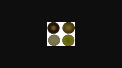
In semiconductor materials, doping is used mainly for controlling the electrical properties. There have been attempts to grow low‐resistivity n‐type gallium nitride (GaN) crystals by doping oxygen, germanium, and silicon, because a low‐resistivity GaN substrate is required to reduce the power losses of optical and electrical devices. However, in those efforts, the crystal color turns black with the increase in the concentration of the n‐type additives, even though they are shallow donors. Herein, it is explained why heavily doped n‐type GaN crystals exhibit low transparency. From optical absorption profiles, the appearance of a band tail from the band edge to 1.5 eV is observed. Considering the band tail theory and our observations, it is concluded that Ga vacancy or Ga vacancy complexes behaving as acceptors induce the band tail and the black color. It is proposed that neutralizing the high charge of defects ensures that low‐colored GaN crystals with low resistivity can be obtained. Moreover, the fabrication of low‐resistivity wafers sliced from a large crystal with a laser produces inexpensive wafers and allows the spread of high‐efficiency GaN devices fabricated on low‐resistivity substrates for saving electric power.
中文翻译:

重掺杂 n 型 GaN 晶体中黑色的成因
在半导体材料中,掺杂主要用于控制电性能。人们尝试通过掺杂氧、锗和硅来生长低电阻率 n 型氮化镓 (GaN) 晶体,因为需要低电阻率 GaN 衬底来减少光学和电学器件的功率损耗。然而,在这些努力中,随着n型添加剂浓度的增加,晶体颜色变黑,即使它们是浅施主。在此,解释了为什么重掺杂的n型GaN晶体表现出低透明度。从光学吸收曲线中,观察到从带边缘到 1.5 eV 的带尾的出现。考虑到带尾理论和我们的观察,得出的结论是,Ga 空位或 Ga 空位配合物作为受体导致了带尾和黑色。提出中和缺陷的高电荷可确保获得低电阻率的浅色 GaN 晶体。此外,用激光从大晶体上切片制造低电阻率晶圆可以生产廉价的晶圆,并允许在低电阻率衬底上制造高效 GaN 器件以节省电力。
更新日期:2024-03-16
中文翻译:
重掺杂 n 型 GaN 晶体中黑色的成因
在半导体材料中,掺杂主要用于控制电性能。人们尝试通过掺杂氧、锗和硅来生长低电阻率 n 型氮化镓 (GaN) 晶体,因为需要低电阻率 GaN 衬底来减少光学和电学器件的功率损耗。然而,在这些努力中,随着n型添加剂浓度的增加,晶体颜色变黑,即使它们是浅施主。在此,解释了为什么重掺杂的n型GaN晶体表现出低透明度。从光学吸收曲线中,观察到从带边缘到 1.5 eV 的带尾的出现。考虑到带尾理论和我们的观察,得出的结论是,Ga 空位或 Ga 空位配合物作为受体导致了带尾和黑色。提出中和缺陷的高电荷可确保获得低电阻率的浅色 GaN 晶体。此外,用激光从大晶体上切片制造低电阻率晶圆可以生产廉价的晶圆,并允许在低电阻率衬底上制造高效 GaN 器件以节省电力。


 京公网安备 11010802027423号