当前位置:
X-MOL 学术
›
Microelectron. Eng.
›
论文详情
Our official English website, www.x-mol.net, welcomes your feedback! (Note: you will need to create a separate account there.)
Fabrication of nanoscale stencils through focused ion beam milling and dry transfer of silicon-on-nothing membrane with perforations
Microelectronic Engineering ( IF 2.3 ) Pub Date : 2024-03-14 , DOI: 10.1016/j.mee.2024.112172 Taeyeong Kim , Jungchul Lee
Microelectronic Engineering ( IF 2.3 ) Pub Date : 2024-03-14 , DOI: 10.1016/j.mee.2024.112172 Taeyeong Kim , Jungchul Lee
|
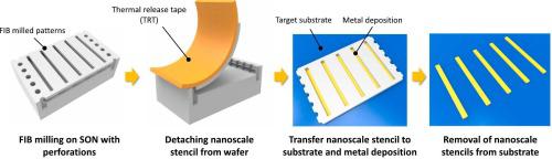
Nanoscale stencil lithography, providing sub-micrometer resolutions, is being implemented as a reliable patterning technique within the nanotechnology domain. Despite their advantages such as no resist processing, easy manipulation and reusability, patterning using a nanoscale stencil often faces challenges due to the gap between the nanoscale stencil and the substrate. This tends to result in unwanted pattern blurring, typically dimension wider than intended design. To address this issue, we minimize the gap by conformally attaching the nanoscale stencil to the substrate, thereby effectively eliminating a key factor contributing to the blurring effect. The nanoscale stencil is fabricated by forming nanoslits on the 50 nm thick Silicon-on-Nothing (SON) membrane with perforations, using focused ion beam (FIB) milling. The transfer of this stencil onto a substrate enables conformal adhesion due to its 10 times lower flexural rigidity of the stencil compared to bulk silicon. Upon deposition of chromium and gold through the transferred stencil, a metal pattern array with the full width at half maximum (FWHM) of 43 nm is produced, demonstrating the potential of our approach for fabricating uniform nanoscale patterns with enhanced pattern resolution.
中文翻译:

通过聚焦离子束铣削和带穿孔的无硅膜干转移来制造纳米级模板
纳米级模板光刻可提供亚微米分辨率,正在纳米技术领域作为一种可靠的图案化技术来实施。尽管纳米级模板具有无需抗蚀剂处理、易于操作和可重复使用等优点,但由于纳米级模板和基板之间存在间隙,使用纳米级模板进行图案化常常面临挑战。这往往会导致不必要的图案模糊,通常尺寸比预期设计宽。为了解决这个问题,我们通过将纳米级模板共形地附着到基板上来最小化间隙,从而有效地消除导致模糊效果的关键因素。该纳米级模板是通过使用聚焦离子束 (FIB) 铣削在 50 nm 厚的带穿孔的无硅 (SON) 膜上形成纳米狭缝而制成的。由于该模板的弯曲刚度比体硅低 10 倍,因此将该模板转移到基板上可实现保形粘合。通过转移模板沉积铬和金后,产生半峰全宽 (FWHM) 为 43 nm 的金属图案阵列,这证明了我们的方法在制造具有增强图案分辨率的均匀纳米级图案方面的潜力。
更新日期:2024-03-14
中文翻译:
通过聚焦离子束铣削和带穿孔的无硅膜干转移来制造纳米级模板
纳米级模板光刻可提供亚微米分辨率,正在纳米技术领域作为一种可靠的图案化技术来实施。尽管纳米级模板具有无需抗蚀剂处理、易于操作和可重复使用等优点,但由于纳米级模板和基板之间存在间隙,使用纳米级模板进行图案化常常面临挑战。这往往会导致不必要的图案模糊,通常尺寸比预期设计宽。为了解决这个问题,我们通过将纳米级模板共形地附着到基板上来最小化间隙,从而有效地消除导致模糊效果的关键因素。该纳米级模板是通过使用聚焦离子束 (FIB) 铣削在 50 nm 厚的带穿孔的无硅 (SON) 膜上形成纳米狭缝而制成的。由于该模板的弯曲刚度比体硅低 10 倍,因此将该模板转移到基板上可实现保形粘合。通过转移模板沉积铬和金后,产生半峰全宽 (FWHM) 为 43 nm 的金属图案阵列,这证明了我们的方法在制造具有增强图案分辨率的均匀纳米级图案方面的潜力。


 京公网安备 11010802027423号