当前位置:
X-MOL 学术
›
Phys. Status Solidi B
›
论文详情
Our official English website, www.x-mol.net, welcomes your feedback! (Note: you will need to create a separate account there.)
Two‐Dimensional Characterization of Au/Ni/Thin Heavily‐Mg‐Doped p‐/n‐GaN Structure under Applied Voltage by Scanning Internal Photoemission Microscopy
Physica Status Solidi (B) - Basic Solid State Physics ( IF 1.6 ) Pub Date : 2024-03-19 , DOI: 10.1002/pssb.202400033 Hiroki Imabayashi 1 , Haruto Yoshimura 1 , Fumimasa Horikiri 2 , Yoshinobu Narita 2 , Hajime Fujikura 2 , Hiroshi Ohta 3 , Tomoyoshi Mishima 3 , Kenji Shiojima 1
Physica Status Solidi (B) - Basic Solid State Physics ( IF 1.6 ) Pub Date : 2024-03-19 , DOI: 10.1002/pssb.202400033 Hiroki Imabayashi 1 , Haruto Yoshimura 1 , Fumimasa Horikiri 2 , Yoshinobu Narita 2 , Hajime Fujikura 2 , Hiroshi Ohta 3 , Tomoyoshi Mishima 3 , Kenji Shiojima 1
Affiliation
|
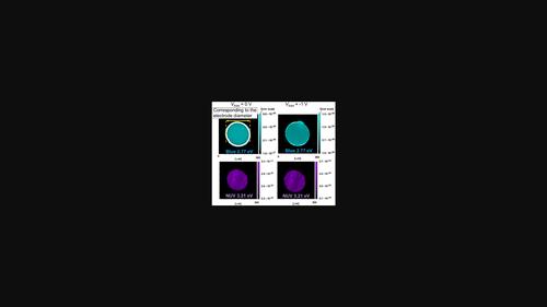
The two‐dimensional characterization of the Au/Ni/thin p+ ‐GaN/n− ‐GaN structure, which is a part of a junction barrier Schottky structure, is demonstrated by scanning internal photoemission microscopy (SIPM) method. In the SIPM photoyield image using a blue laser, small photocurrents based on the internal photoemission effect by electron injection across the metal/semiconductor interface (from Ni to GaN) are detected in the center of the electrode. On the periphery, large photocurrents in the opposite direction are detected. These currents are caused by the hole injection from Ni into p+ ‐GaN layer and the electrical field in the laterally extended depletion layer at the edge. By using a violet laser, large photocurrents based on the fundamental absorption generated in the depletion layer of the n− ‐GaN layer are uniformly detected over the electrode. It is conformed that SIPM can be available for quasi‐three‐dimensional characterization of this structure.
中文翻译:

通过扫描内部光电显微镜对外加电压下 Au/Ni/薄重镁掺杂 p-/n-GaN 结构进行二维表征
Au/Ni/薄 p 的二维表征+ ‐GaN/n- ‐GaN 结构是结势垒肖特基结构的一部分,通过扫描内部光电显微镜 (SIPM) 方法进行了演示。在使用蓝色激光的 SIPM 光产率图像中,在电极中心检测到基于跨金属/半导体界面(从 Ni 到 GaN)的电子注入产生的内部光电发射效应的小光电流。在外围,检测到相反方向的大光电流。这些电流是由 Ni 到 p 的空穴注入引起的+ ‐GaN层和边缘横向延伸的耗尽层中的电场。通过使用紫激光,基于n耗尽层中产生的基本吸收的大光电流- ‐GaN 层在电极上均匀检测到。一致认为SIPM可用于该结构的准三维表征。
更新日期:2024-03-19
中文翻译:
通过扫描内部光电显微镜对外加电压下 Au/Ni/薄重镁掺杂 p-/n-GaN 结构进行二维表征
Au/Ni/薄 p 的二维表征


 京公网安备 11010802027423号