当前位置:
X-MOL 学术
›
Phys. Rev. Materials
›
论文详情
Our official English website, www.x-mol.net, welcomes your feedback! (Note: you will need to create a separate account there.)
Thin film growth of the Weyl semimetal NbAs
Physical Review Materials ( IF 3.4 ) Pub Date : 2024-03-22 , DOI: 10.1103/physrevmaterials.8.034204 Wilson Yánez-Parreño , Yu-Sheng Huang , Supriya Ghosh , Saurav Islam , Javier E. Gómez , Emma Steinebronn , Anthony Richardella , Luis Avilés-Félix , Alejandro Butera , K. Andre Mkhoyan , Nitin Samarth
Physical Review Materials ( IF 3.4 ) Pub Date : 2024-03-22 , DOI: 10.1103/physrevmaterials.8.034204 Wilson Yánez-Parreño , Yu-Sheng Huang , Supriya Ghosh , Saurav Islam , Javier E. Gómez , Emma Steinebronn , Anthony Richardella , Luis Avilés-Félix , Alejandro Butera , K. Andre Mkhoyan , Nitin Samarth
|
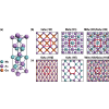
We report the synthesis and characterization of thin films of the Weyl semimetal NbAs grown on GaAs (100) and As-terminated GaAs (111)B substrates. By choosing the appropriate substrate, we can stabilize the growth of NbAs in the [001] and [100] directions. We combine x-ray characterization with high-angle annular dark field scanning transmission electron microscopy to understand both the macroscopic and microscopic structure of the NbAs thin films. We show that these films are textured with domains that are tens of nanometers in size and that, on a macroscopic scale, are mostly aligned to a single crystalline direction. We describe electrical transport measurements that reveal similar behavior in films grown in both crystalline orientations, namely resistivity in the range and carrier densities in the range at 2 K. Finally we measure spin to charge conversion in NbAs and show that it qualitatively agrees with first principles calculations.
中文翻译:

外尔半金属 NbAs 薄膜生长
我们报告了在 GaAs (100) 和 As 端接的 GaAs (111)B 衬底上生长的 Weyl 半金属 NbAs 薄膜的合成和表征。通过选择合适的衬底,我们可以稳定NbAs在[001]和[100]方向上的生长。我们将 X 射线表征与高角度环形暗场扫描透射电子显微镜相结合,以了解 NbAs 薄膜的宏观和微观结构。我们表明,这些薄膜具有数十纳米大小的域纹理,并且在宏观尺度上,大部分与单个晶体方向对齐。我们描述了电传输测量,揭示了在两个晶体方向生长的薄膜中的类似行为,即电阻率范围和范围内的载流子密度最后,我们测量了 NbAs 中的自旋到电荷的转换,并表明它在质量上与第一原理计算一致。
更新日期:2024-03-22
中文翻译:
外尔半金属 NbAs 薄膜生长
我们报告了在 GaAs (100) 和 As 端接的 GaAs (111)B 衬底上生长的 Weyl 半金属 NbAs 薄膜的合成和表征。通过选择合适的衬底,我们可以稳定NbAs在[001]和[100]方向上的生长。我们将 X 射线表征与高角度环形暗场扫描透射电子显微镜相结合,以了解 NbAs 薄膜的宏观和微观结构。我们表明,这些薄膜具有数十纳米大小的域纹理,并且在宏观尺度上,大部分与单个晶体方向对齐。我们描述了电传输测量,揭示了在两个晶体方向生长的薄膜中的类似行为,即电阻率范围和范围内的载流子密度最后,我们测量了 NbAs 中的自旋到电荷的转换,并表明它在质量上与第一原理计算一致。


 京公网安备 11010802027423号