当前位置:
X-MOL 学术
›
Phys. Rev. Materials
›
论文详情
Our official English website, www.x-mol.net, welcomes your feedback! (Note: you will need to create a separate account there.)
Characterization of singlein situprepared interfaces composed of niobium and a selectively grown (Bi1−xSbx)2Te3topological insulator nanoribbon
Physical Review Materials ( IF 3.4 ) Pub Date : 2024-03-22 , DOI: 10.1103/physrevmaterials.8.034205 Kevin Janßen , Philipp Rüßmann , Sergej Liberda , Michael Schleenvoigt , Xiao Hou , Abdur Rehman Jalil , Florian Lentz , Stefan Trellenkamp , Benjamin Bennemann , Erik Zimmermann , Gregor Mussler , Peter Schüffelgen , Claus-Michael Schneider , Stefan Blügel , Detlev Grützmacher , Lukasz Plucinski , Thomas Schäpers
Physical Review Materials ( IF 3.4 ) Pub Date : 2024-03-22 , DOI: 10.1103/physrevmaterials.8.034205 Kevin Janßen , Philipp Rüßmann , Sergej Liberda , Michael Schleenvoigt , Xiao Hou , Abdur Rehman Jalil , Florian Lentz , Stefan Trellenkamp , Benjamin Bennemann , Erik Zimmermann , Gregor Mussler , Peter Schüffelgen , Claus-Michael Schneider , Stefan Blügel , Detlev Grützmacher , Lukasz Plucinski , Thomas Schäpers
|
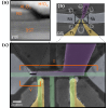
With increasing attention in Majorana physics for possible quantum bit applications, a large interest has been developed to understand the properties of the interface between an -type superconductor and a topological insulator. Up to this point the interface analysis was mainly focused on in situ prepared Josephson junctions, which consist of two coupled single interfaces or to ex situ fabricated single interface devices. In our work we utilize a fabrication process, combining selective area growth and shadow evaporation which allows the characterization of a single in situ fabricated nanointerface. The resulting high interface transparency is apparent by a zero bias conductance increase by a factor of 1.7. Furthermore, we present a comprehensive differential conductance analysis of our single in situ interface for various magnetic fields, temperatures, and gate voltages. Additionally, density functional theory calculations of the superconductor/topological insulator interface are performed in order to explain the peaklike shape of our differential conductance spectra and the origin of the observed smearing of conductance features.
中文翻译:

由铌和选择性生长的 (Bi1−xSbx)2Te3 拓扑绝缘体纳米带组成的单原位制备界面的表征
随着马约拉纳物理学对可能的量子比特应用的日益关注,人们对理解量子比特之间的界面特性产生了很大的兴趣。型超导体和拓扑绝缘体。到目前为止,界面分析主要集中在原位制备的约瑟夫森结,它由两个耦合的单界面或异位制造的单界面器件组成。在我们的工作中,我们利用一种制造工艺,结合选择性区域生长和阴影蒸发,从而可以表征单个原位制造的纳米界面。由此产生的高界面透明度通过零偏压电导增加 1.7 倍来体现。此外,我们还针对各种磁场、温度和栅极电压对单个原位界面进行了全面的微分电导分析。此外,还进行了超导体/拓扑绝缘体界面的密度泛函理论计算,以解释我们的微分电导谱的峰状形状以及观察到的电导特征拖尾的起源。
更新日期:2024-03-22
中文翻译:
由铌和选择性生长的 (Bi1−xSbx)2Te3 拓扑绝缘体纳米带组成的单原位制备界面的表征
随着马约拉纳物理学对可能的量子比特应用的日益关注,人们对理解量子比特之间的界面特性产生了很大的兴趣。型超导体和拓扑绝缘体。到目前为止,界面分析主要集中在原位制备的约瑟夫森结,它由两个耦合的单界面或异位制造的单界面器件组成。在我们的工作中,我们利用一种制造工艺,结合选择性区域生长和阴影蒸发,从而可以表征单个原位制造的纳米界面。由此产生的高界面透明度通过零偏压电导增加 1.7 倍来体现。此外,我们还针对各种磁场、温度和栅极电压对单个原位界面进行了全面的微分电导分析。此外,还进行了超导体/拓扑绝缘体界面的密度泛函理论计算,以解释我们的微分电导谱的峰状形状以及观察到的电导特征拖尾的起源。


 京公网安备 11010802027423号