Nature ( IF 64.8 ) Pub Date : 2024-03-27 , DOI: 10.1038/s41586-024-07243-0 Bosai Lyu , Jiajun Chen , Sen Wang , Shuo Lou , Peiyue Shen , Jingxu Xie , Lu Qiu , Izaac Mitchell , Can Li , Cheng Hu , Xianliang Zhou , Kenji Watanabe , Takashi Taniguchi , Xiaoqun Wang , Jinfeng Jia , Qi Liang , Guorui Chen , Tingxin Li , Shiyong Wang , Wengen Ouyang , Oded Hod , Feng Ding , Michael Urbakh , Zhiwen Shi
|
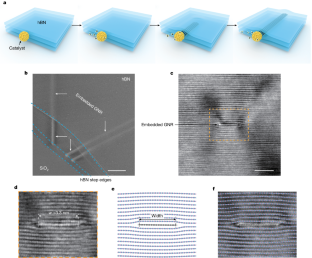
Van der Waals encapsulation of two-dimensional materials in hexagonal boron nitride (hBN) stacks is a promising way to create ultrahigh-performance electronic devices1,2,3,4. However, contemporary approaches for achieving van der Waals encapsulation, which involve artificial layer stacking using mechanical transfer techniques, are difficult to control, prone to contamination and unscalable. Here we report the transfer-free direct growth of high-quality graphene nanoribbons (GNRs) in hBN stacks. The as-grown embedded GNRs exhibit highly desirable features being ultralong (up to 0.25 mm), ultranarrow (<5 nm) and homochiral with zigzag edges. Our atomistic simulations show that the mechanism underlying the embedded growth involves ultralow GNR friction when sliding between AA′-stacked hBN layers. Using the grown structures, we demonstrate the transfer-free fabrication of embedded GNR field-effect devices that exhibit excellent performance at room temperature with mobilities of up to 4,600 cm2 V–1 s–1 and on–off ratios of up to 106. This paves the way for the bottom-up fabrication of high-performance electronic devices based on embedded layered materials.
中文翻译:
在六方氮化硼堆叠中生长的石墨烯纳米带用于高性能电子产品
在六方氮化硼 (hBN) 堆栈中对二维材料进行范德华封装是创建超高性能电子器件的一种有前途的方法1,2,3,4。然而,当代实现范德华封装的方法涉及使用机械转移技术的人工层堆叠,难以控制、容易受到污染且无法扩展。在这里,我们报告了六方氮化硼堆叠中高质量石墨烯纳米带(GNR)的无转移直接生长。生长的嵌入式 GNR 表现出非常理想的特征,即超长(长达 0.25 mm)、超窄(<5 nm)和具有锯齿形边缘的同手性。我们的原子模拟表明,嵌入生长的机制涉及在 AA' 堆叠的六方氮化硼层之间滑动时的超低 GNR 摩擦。使用生长的结构,我们演示了嵌入式 GNR 场效应器件的无转移制造,该器件在室温下表现出优异的性能,迁移率高达 4,600 cm 2 V –1 s –1和高达 10 6的开关比。这为基于嵌入式层状材料的高性能电子器件的自下而上制造铺平了道路。


 京公网安备 11010802027423号