当前位置:
X-MOL 学术
›
Adv. Opt. Mater.
›
论文详情
Our official English website, www.x-mol.net, welcomes your feedback! (Note: you will need to create a separate account there.)
A Dual Mode MoTe2/WS2/WSe2 Double Van der Waals Heterojunctions Phototransistor for Optical Imaging and Communication
Advanced Optical Materials ( IF 9 ) Pub Date : 2024-04-04 , DOI: 10.1002/adom.202400023 Zhongming Li 1, 2 , Tao Zheng 1 , Mengmeng Yang 1 , Yiming Sun 1 , Dongxiang Luo 3 , Wei Gao 1 , Zhaoqiang Zheng 2 , Jingbo Li 4
Advanced Optical Materials ( IF 9 ) Pub Date : 2024-04-04 , DOI: 10.1002/adom.202400023 Zhongming Li 1, 2 , Tao Zheng 1 , Mengmeng Yang 1 , Yiming Sun 1 , Dongxiang Luo 3 , Wei Gao 1 , Zhaoqiang Zheng 2 , Jingbo Li 4
Affiliation
|
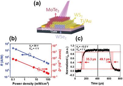
Van der Waals (vdW) heterostructures, formed by stacking different two‐dimensional (2D) materials, have emerged as a promising platform for next‐generation optoelectronic devices through band engineering. While various all‐2D and mixed‐dimensional heterojunction phototransistors based on p–n junctions or Schottky junctions have been developed, their performance, often constrained by the trade‐off between responsivity (R ) and response speed, limits their widespread application. Here, a dual‐mode phototransistor based on a MoTe2 /WS2 /WSe2 double vdW heterostructure is designed. The bottom WSe2 layer effectively modulates the entire MoTe2 /WS2 heterojunction channel, enabling both photoconductive and photovoltaic modes with exceptional optoelectronic properties in a single device. Specifically, the proposed device exhibits a maximum R of 2540 A W−1 and an impressive specific detectivity of 8 × 10¹² Jones under the photoconductive mode. Under the photovoltaic mode, it achieves a fast response speed of 35.3/49.1 µs and a high light on/off ratio of 2 × 10⁵ . Additionally, the device exhibits latent potential for high‐resolution imaging across various wavelengths and fast optical communication. This work offers a rational alternative for achieving dual‐mode photodetection and highlights its promising application prospects in imaging and optical communication.
中文翻译:

用于光学成像和通信的双模 MoTe2/WS2/WSe2 双范德华异质结光电晶体管
通过堆叠不同的二维(2D)材料形成的范德华(vdW)异质结构已成为通过能带工程开发下一代光电器件的有前景的平台。虽然已经开发出基于 p-n 结或肖特基结的各种全二维和混合维异质结光电晶体管,但它们的性能通常受到响应度之间的权衡(右 )和响应速度,限制了它们的广泛应用。这里,基于 MoTe 的双模光电晶体管2 /WS2 /硒化钨2 设计了双vdW异质结构。底部WSe2 层有效地调制整个MoTe2 /WS2 异质结通道,在单个器件中实现光电导和光伏模式,并具有出色的光电特性。具体来说,所提出的设备表现出最大右 2540 秋冬季节−1 以及令人印象深刻的 8 × 10 比探测率12 光电导模式下的琼斯。光伏模式下,实现35.3/49.1 µs的快速响应速度和2×10的高开灯比5 。此外,该设备还展现出跨各种波长的高分辨率成像和快速光通信的潜在潜力。这项工作为实现双模光电探测提供了一种合理的替代方案,并凸显了其在成像和光通信方面的广阔应用前景。
更新日期:2024-04-04
中文翻译:
用于光学成像和通信的双模 MoTe2/WS2/WSe2 双范德华异质结光电晶体管
通过堆叠不同的二维(2D)材料形成的范德华(vdW)异质结构已成为通过能带工程开发下一代光电器件的有前景的平台。虽然已经开发出基于 p-n 结或肖特基结的各种全二维和混合维异质结光电晶体管,但它们的性能通常受到响应度之间的权衡(


 京公网安备 11010802027423号