当前位置:
X-MOL 学术
›
Laser Photonics Rev.
›
论文详情
Our official English website, www.x-mol.net, welcomes your feedback! (Note: you will need to create a separate account there.)
Fiber–Chip–Fiber Mode/Polarization/Wavelength Transmission and Processing with Few‐Mode Fiber, (de)Multiplexing SiO2 Chip and ROADM Si Chip
Laser & Photonics Reviews ( IF 11.0 ) Pub Date : 2024-04-05 , DOI: 10.1002/lpor.202300489 Kang Li 1, 2 , Chengkun Cai 1, 2 , Xiaoping Cao 1, 2 , Min Yang 1, 2 , Guofeng Yan 1, 2 , Yuanjian Wan 1, 2 , Guangze Wu 1, 2 , Kangrui Wang 1, 2 , Jian Wang 1, 2
Laser & Photonics Reviews ( IF 11.0 ) Pub Date : 2024-04-05 , DOI: 10.1002/lpor.202300489 Kang Li 1, 2 , Chengkun Cai 1, 2 , Xiaoping Cao 1, 2 , Min Yang 1, 2 , Guofeng Yan 1, 2 , Yuanjian Wan 1, 2 , Guangze Wu 1, 2 , Kangrui Wang 1, 2 , Jian Wang 1, 2
Affiliation
|
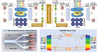
The emergence of optical communications has opened up new perspectives for high‐capacity data transmission and signal processing, to meet the demand of the increasing data traffic. Despite significant progress in multi‐dimensional multiplexing for capacity scaling in fiber–optic communications or photonic networks‐on‐chip, achieving high‐capacity data transmission and signal processing in an entire fiber–chip–fiber system remains a great challenge. This challenge is attributed to the lack of effective multi‐dimensional coupling between fiber and chip. Here, the 3D (de)multiplexing SiO2 chip inscribed by femtosecond laser direct writing is proposed to achieve the multi‐dimensional coupling between the few‐mode fiber (FMF) transmission link and the silicon processing network. Combined with the 2D silicon chip fabricated by a standard lithography process, a multi‐dimensional fiber–chip–fiber communication system designed to transmit and process the hybrid wavelength‐, mode‐ and polarization‐division multiplexing signals in FMF is constructed. The silicon chip integrates Mach–Zehnder interferometer (MZI) switches and arrayed‐waveguide gratings (AWGs) to serve as a reconfigurable optical add/drop multiplexer (ROADM). As a proof‐of‐concept demonstration, a 96‐channel FMF–chip–FMF communication system with a data transmission capacity of 4.032 Tbit s−1 , achieving a bit‐error ratio (BER) of less than 3.8 × 10⁻³ , is successfully implemented.
中文翻译:

光纤-芯片-光纤模式/偏振/波长传输和少模光纤处理、(解)复用 SiO2 芯片和 ROADM Si 芯片
光通信的出现为大容量数据传输和信号处理开辟了新的前景,以满足不断增长的数据流量的需求。尽管在光纤通信或片上光子网络的容量扩展方面多维复用取得了重大进展,但在整个光纤-芯片-光纤系统中实现高容量数据传输和信号处理仍然是一个巨大的挑战。这一挑战归因于光纤和芯片之间缺乏有效的多维耦合。这里,3D(解)复用 SiO2 提出了飞秒激光直写刻写芯片,以实现少模光纤(FMF)传输链路与硅加工网络之间的多维耦合。结合标准光刻工艺制造的二维硅芯片,构建了一个多维光纤-芯片-光纤通信系统,用于传输和处理FMF中的混合波长、模式和偏振复用信号。该硅芯片集成了马赫-曾德干涉仪 (MZI) 开关和阵列波导光栅 (AWG),用作可重构光学分插复用器 (ROADM)。作为概念验证演示,数据传输容量为 4.032 Tbit s 的 96 通道 FMF-芯片-FMF 通信系统−1 ,误码率 (BER) 小于 3.8 × 10⁻³ ,已成功实施。
更新日期:2024-04-05
中文翻译:
光纤-芯片-光纤模式/偏振/波长传输和少模光纤处理、(解)复用 SiO2 芯片和 ROADM Si 芯片
光通信的出现为大容量数据传输和信号处理开辟了新的前景,以满足不断增长的数据流量的需求。尽管在光纤通信或片上光子网络的容量扩展方面多维复用取得了重大进展,但在整个光纤-芯片-光纤系统中实现高容量数据传输和信号处理仍然是一个巨大的挑战。这一挑战归因于光纤和芯片之间缺乏有效的多维耦合。这里,3D(解)复用 SiO


 京公网安备 11010802027423号