当前位置:
X-MOL 学术
›
Adv. Funct. Mater.
›
论文详情
Our official English website, www.x-mol.net, welcomes your feedback! (Note: you will need to create a separate account there.)
Domains with Varying Conductance in Tensile Strained SrMnO3 Thin Films Using Out‐of‐Plane Electric Fields
Advanced Functional Materials ( IF 19.0 ) Pub Date : 2024-04-16 , DOI: 10.1002/adfm.202404150 Job J. L. van Rijn 1 , Ishitro Bhaduri 1 , Majid Ahmadi 1 , Beatriz Noheda 1 , Bart J. Kooi 1 , Tamalika Banerjee 1
Advanced Functional Materials ( IF 19.0 ) Pub Date : 2024-04-16 , DOI: 10.1002/adfm.202404150 Job J. L. van Rijn 1 , Ishitro Bhaduri 1 , Majid Ahmadi 1 , Beatriz Noheda 1 , Bart J. Kooi 1 , Tamalika Banerjee 1
Affiliation
|
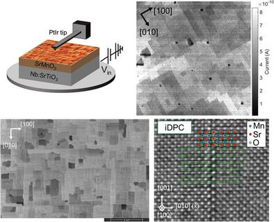
Domains and domain wall engineering have been extensively explored in ferroic materials for a wide range of applications in nanoelectronics and spintronics. Complex oxides exhibiting strongly correlated properties are model platforms for such studies where response to strain or external stimuli such as electric field, temperature and light can be probed. Here, domains in strained SrMnO3 films, grown on a degenerate semiconductor, allowing for conduction in an out‐of‐plane geometry, are studied using a combination of microscopy probes. Using conductive atomic force microscopy, electrically isolated domains with varying conductance are found and their temporal evolution is investigated. Further, their formation and microstructure are studied using scanning transmission electron microscopy and secondary electron contrast in scanning electron microscopy. An important contribution is establishing that the observed domains are formed by cracks, driven by inhomogeneous strain relaxation throughout the film, resulting in significantly high strain planes. The potential of secondary electrons to detect domain dependent contrast over a large area, ensuing due to the use of a degenerate semiconductor correlates with the conductive properties of the domains and serves as a new direction to probe domains and domain walls in ferroic materials.
中文翻译:

使用面外电场在拉伸应变 SrMnO3 薄膜中具有不同电导的域
铁磁材料中的磁畴和磁畴壁工程已得到广泛探索,在纳米电子学和自旋电子学中具有广泛的应用。表现出强相关特性的复合氧化物是此类研究的模型平台,可以探测对应变或外部刺激(例如电场、温度和光)的响应。这里,应变 SrMnO 中的域3 使用显微镜探针的组合来研究在简并半导体上生长的薄膜,允许在平面外几何形状中传导。使用导电原子力显微镜,发现了具有不同电导的电隔离域,并研究了它们的时间演化。此外,使用扫描透射电子显微镜和扫描电子显微镜中的二次电子对比研究了它们的形成和微观结构。一个重要的贡献是确定观察到的域是由裂纹形成的,裂纹是由整个薄膜的不均匀应变松弛驱动的,导致显着高的应变平面。由于简并半导体的使用,二次电子在大面积上检测与磁畴相关的对比度的潜力与磁畴的导电特性相关,并成为探测铁质材料中磁畴和磁畴壁的新方向。
更新日期:2024-04-16
中文翻译:
使用面外电场在拉伸应变 SrMnO3 薄膜中具有不同电导的域
铁磁材料中的磁畴和磁畴壁工程已得到广泛探索,在纳米电子学和自旋电子学中具有广泛的应用。表现出强相关特性的复合氧化物是此类研究的模型平台,可以探测对应变或外部刺激(例如电场、温度和光)的响应。这里,应变 SrMnO 中的域


 京公网安备 11010802027423号