当前位置:
X-MOL 学术
›
Nanoscale Adv.
›
论文详情
Our official English website, www.x-mol.net, welcomes your feedback! (Note: you will need to create a separate account there.)
On the structural evolution of nanoporous optically transparent CuO photocathodes upon calcination for photoelectrochemical applications
Nanoscale Advances ( IF 4.7 ) Pub Date : 2024-04-19 , DOI: 10.1039/d4na00199k Lukas Korell 1 , Stefan Lauterbach 2 , Jana Timm 3 , Li Wang 4 , Maximilian Mellin 1 , Anna Kundmann 4 , Qingyang Wu 1 , Chuanmu Tian 1 , Roland Marschall 3 , Jan P. Hofmann 1 , Frank E. Osterloh 4 , Marcus Einert 1
Nanoscale Advances ( IF 4.7 ) Pub Date : 2024-04-19 , DOI: 10.1039/d4na00199k Lukas Korell 1 , Stefan Lauterbach 2 , Jana Timm 3 , Li Wang 4 , Maximilian Mellin 1 , Anna Kundmann 4 , Qingyang Wu 1 , Chuanmu Tian 1 , Roland Marschall 3 , Jan P. Hofmann 1 , Frank E. Osterloh 4 , Marcus Einert 1
Affiliation
|
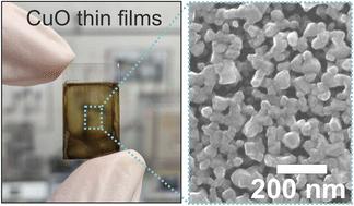
Copper oxides are promising photocathode materials for solar hydrogen production due to their narrow optical band gap energy allowing broad visible light absorption. However, they suffer from severe photocorrosion upon illumination, mainly due to copper reduction. Nanostructuring has been proven to enhance the photoresponse of CuO photocathodes; however, there is a lack of precise structural control on the nanoscale upon sol–gel synthesis and calcination for achieving optically transparent CuO thin film photoabsorbers. In this study, nanoporous and nanocrystalline CuO networks were prepared by a soft-templating and dip-coating method utilizing poly(ethylene oxide)-block-poly(propylene oxide)-block-poly(ethylene oxide) (Pluronic® F-127) as a structure-directing agent, resulting for the first-time in uniformly structured, crack-free, and optically transparent CuO thin films. The photoelectrochemical properties of the nanoporous CuO frameworks were investigated as a function of the calcination temperature and film thickness, revealing important information about the photocurrent, photostability, and photovoltage. Based on surface photovoltage spectroscopy (SPV), the films are p-type and generate up to 60 mV photovoltage at 2.0 eV (0.050 mW cm−2) irradiation for the film annealed at 750 °C. For these high annealing temperatures, the nanocrystalline domains in the thin film structure are more developed, resulting in improved electronic quality. In aqueous electrolytes with or without methyl viologen (as a fast electron acceptor), CuO films show cathodic photocurrents of up to −2.4 mA cm−2 at 0.32 V vs. RHE (air mass (AM) 1.5). However, the photocurrents were found to be entirely due to photocorrosion of the films and decay to near zero over the course of 20 min under AM 1.5 illumination. These fundamental results on the structural and morphological development upon calcination provide a direction and show the necessity for further (surface) treatment of sol–gel derived CuO photocathodes for photoelectrochemical applications. The study demonstrates how to control the size of nanopores starting from mesopore formation at 400 °C to the evolution of macroporous frameworks at 750 °C.
中文翻译:

用于光电化学应用的纳米多孔光学透明 CuO 光电阴极在煅烧后的结构演变
铜氧化物由于其窄光学带隙能量允许广泛的可见光吸收,是用于太阳能制氢的有前途的光电阴极材料。然而,它们在光照下会遭受严重的光腐蚀,这主要是由于铜的还原。纳米结构已被证明可以增强 CuO 光电阴极的光响应;然而,在溶胶-凝胶合成和煅烧过程中,缺乏对纳米尺度的精确结构控制来实现光学透明的 CuO 薄膜光吸收器。在这项研究中,利用聚(环氧乙烷)-嵌段-聚(环氧丙烷)-嵌段-聚(环氧乙烷)(Pluronic® F-127)通过软模板和浸涂方法制备了纳米多孔和纳米晶体 CuO 网络。作为结构导向剂,首次产生结构均匀、无裂纹且光学透明的 CuO 薄膜。研究了纳米多孔 CuO 框架的光电化学性质与煅烧温度和膜厚度的函数关系,揭示了有关光电流、光稳定性和光电压的重要信息。基于表面光电压光谱(SPV),这些薄膜是p型的,并且在750℃退火的薄膜在2.0eV(0.050mWcm -2 )照射下产生高达60mV的光电压。对于这些高退火温度,薄膜结构中的纳米晶域更加发达,从而提高了电子质量。在含有或不含甲基紫精(作为快速电子受体)的水性电解质中,CuO 薄膜在 0.32 V vs. RHE(空气质量 (AM) 1.5)下表现出高达 -2.4 mA cm -2的阴极光电流。然而,发现光电流完全是由于薄膜的光腐蚀造成的,并且在 AM 1.5 照明下在 20 分钟内衰减到接近于零。这些关于煅烧后结构和形态发展的基本结果为光电化学应用提供了方向,并表明了对溶胶-凝胶衍生的 CuO 光阴极进行进一步(表面)处理的必要性。该研究展示了如何控制纳米孔的尺寸,从 400 °C 的介孔形成到 750 °C 的大孔框架的演变。
更新日期:2024-04-19
中文翻译:
用于光电化学应用的纳米多孔光学透明 CuO 光电阴极在煅烧后的结构演变
铜氧化物由于其窄光学带隙能量允许广泛的可见光吸收,是用于太阳能制氢的有前途的光电阴极材料。然而,它们在光照下会遭受严重的光腐蚀,这主要是由于铜的还原。纳米结构已被证明可以增强 CuO 光电阴极的光响应;然而,在溶胶-凝胶合成和煅烧过程中,缺乏对纳米尺度的精确结构控制来实现光学透明的 CuO 薄膜光吸收器。在这项研究中,利用聚(环氧乙烷)-嵌段-聚(环氧丙烷)-嵌段-聚(环氧乙烷)(Pluronic® F-127)通过软模板和浸涂方法制备了纳米多孔和纳米晶体 CuO 网络。作为结构导向剂,首次产生结构均匀、无裂纹且光学透明的 CuO 薄膜。研究了纳米多孔 CuO 框架的光电化学性质与煅烧温度和膜厚度的函数关系,揭示了有关光电流、光稳定性和光电压的重要信息。基于表面光电压光谱(SPV),这些薄膜是p型的,并且在750℃退火的薄膜在2.0eV(0.050mWcm -2 )照射下产生高达60mV的光电压。对于这些高退火温度,薄膜结构中的纳米晶域更加发达,从而提高了电子质量。在含有或不含甲基紫精(作为快速电子受体)的水性电解质中,CuO 薄膜在 0.32 V vs. RHE(空气质量 (AM) 1.5)下表现出高达 -2.4 mA cm -2的阴极光电流。然而,发现光电流完全是由于薄膜的光腐蚀造成的,并且在 AM 1.5 照明下在 20 分钟内衰减到接近于零。这些关于煅烧后结构和形态发展的基本结果为光电化学应用提供了方向,并表明了对溶胶-凝胶衍生的 CuO 光阴极进行进一步(表面)处理的必要性。该研究展示了如何控制纳米孔的尺寸,从 400 °C 的介孔形成到 750 °C 的大孔框架的演变。


 京公网安备 11010802027423号