当前位置:
X-MOL 学术
›
ACS Photonics
›
论文详情
Our official English website, www.x-mol.net, welcomes your feedback! (Note: you will need to create a separate account there.)
GaN/InGaN LED Sidewall Defects Analysis by Cathodoluminescence and Photosensitive Kelvin Probe Force Microscopy
ACS Photonics ( IF 7 ) Pub Date : 2024-04-20 , DOI: 10.1021/acsphotonics.4c00384 Palmerina González-Izquierdo 1 , Névine Rochat 1 , Konrad Sakowski 2, 3 , Davide Zoccarato 1 , Matthew Charles 1 , Łukasz Borowik 1
ACS Photonics ( IF 7 ) Pub Date : 2024-04-20 , DOI: 10.1021/acsphotonics.4c00384 Palmerina González-Izquierdo 1 , Névine Rochat 1 , Konrad Sakowski 2, 3 , Davide Zoccarato 1 , Matthew Charles 1 , Łukasz Borowik 1
Affiliation
|
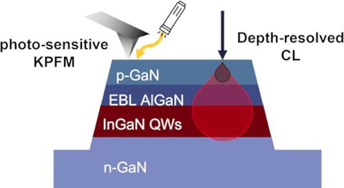
This paper delves into the impact of sidewall defects on a GaN/InGaN epi-LED, utilizing advanced analytical techniques with nanometric resolution: cathodoluminescence (CL) and photosensitive Kelvin probe force microscopy (KPFM). CL investigations at varying excitation energies enable an in-depth study of the epi-LED by distinctly probing the top p-GaN layer and InGaN quantum wells within the mesa structure. These measurements permit the analysis of the impact of sidewall defects on the light-emitting diode (LED) light emission in different epilayers, shedding light on the phenomena affecting LED optoelectronic properties. The results reveal reduced intensities related to the GaN near-band-edge (NBE) and InGaN quantum well emission, along with an increased yellow luminescence band near the mesa edge, attributed to sidewall defects induced during the etching process. Conversely, the top p-GaN layer shows no NBE band and uniform ultraviolet luminescence line (UVL) related to MgGa acceptors, suggesting no effect from sidewall defects. Similarly, the surface photovoltage (SPV) measured on the top p-GaN surface by KPFM shows no significant changes near the mesa boundary. Moreover, KPFM measurements show a slow SPV decay after illumination, indicating charge trapping of holes in the surface of p-GaN, as evidenced by positive SPV and consistent with the simulations. We attribute the absence of the sidewall defects effect and the charge trapping in the p-GaN layer to high-density Mg-related defects, as supported by the uniform CL UVL emission. To ensure that sidewall defects were not masked by the high concentration of Mg impurities, we conducted photosensitive KPFM at low temperatures. At these temperatures, defects are “frozen”, and different types of defects exhibit distinct detrapping time scales. The consistent behavior observed at both the center and border of the mesa structure across three different temperatures confirms that only one type of defect associated with Mg doping rather than sidewall defects is being observed. These findings suggest that the etching process used in LED fabrication does not significantly impact the role of the top p-GaN layer in LED miniaturization. Moreover, they provide crucial insights into defect-induced processes and their influence on device performance, particularly in the vicinity of LED edges. Understanding these effects is essential for fabricating high-performance microLEDs.
中文翻译:

通过阴极发光和光敏开尔文探针力显微镜分析 GaN/InGaN LED 侧壁缺陷
本文利用具有纳米分辨率的先进分析技术:阴极发光 (CL) 和光敏开尔文探针力显微镜 (KPFM),深入研究了侧壁缺陷对 GaN/InGaN Epi-LED 的影响。在不同的激发能量下进行 CL 研究,通过清楚地探测台面结构内的顶部 p-GaN 层和 InGaN 量子阱,能够对 Epi-LED 进行深入研究。这些测量可以分析侧壁缺陷对不同外延层中发光二极管 (LED) 发光的影响,揭示影响 LED 光电特性的现象。结果表明,与 GaN 近带边缘 (NBE) 和 InGaN 量子阱发射相关的强度降低,以及台面边缘附近黄色发光带的增加,这归因于蚀刻过程中引起的侧壁缺陷。相反,顶部 p-GaN 层没有显示出与 Mg Ga受主相关的 NBE 能带和均匀紫外发光线 (UVL) ,表明侧壁缺陷没有影响。同样,通过 KPFM 在顶部 p-GaN 表面上测量的表面光电压 (SPV) 显示台面边界附近没有显着变化。此外,KPFM 测量显示光照后 SPV 衰减缓慢,表明 p-GaN 表面存在空穴电荷俘获,正 SPV 证明了这一点,并且与模拟一致。我们将 p-GaN 层中不存在侧壁缺陷效应和电荷俘获归因于高密度 Mg 相关缺陷,这一点得到了均匀 CL UVL 发射的支持。为了确保侧壁缺陷不被高浓度的Mg杂质掩盖,我们在低温下进行了光敏KPFM。在这些温度下,缺陷被“冻结”,并且不同类型的缺陷表现出不同的去捕获时间尺度。在三种不同温度下在台面结构的中心和边界观察到的一致行为证实,只观察到一种与镁掺杂相关的缺陷,而不是侧壁缺陷。这些发现表明,LED 制造中使用的蚀刻工艺不会显着影响顶部 p-GaN 层在 LED 小型化中的作用。此外,它们还提供了关于缺陷引发的工艺及其对器件性能影响的重要见解,特别是在 LED 边缘附近。了解这些效应对于制造高性能 microLED 至关重要。
更新日期:2024-04-25
中文翻译:
通过阴极发光和光敏开尔文探针力显微镜分析 GaN/InGaN LED 侧壁缺陷
本文利用具有纳米分辨率的先进分析技术:阴极发光 (CL) 和光敏开尔文探针力显微镜 (KPFM),深入研究了侧壁缺陷对 GaN/InGaN Epi-LED 的影响。在不同的激发能量下进行 CL 研究,通过清楚地探测台面结构内的顶部 p-GaN 层和 InGaN 量子阱,能够对 Epi-LED 进行深入研究。这些测量可以分析侧壁缺陷对不同外延层中发光二极管 (LED) 发光的影响,揭示影响 LED 光电特性的现象。结果表明,与 GaN 近带边缘 (NBE) 和 InGaN 量子阱发射相关的强度降低,以及台面边缘附近黄色发光带的增加,这归因于蚀刻过程中引起的侧壁缺陷。相反,顶部 p-GaN 层没有显示出与 Mg Ga受主相关的 NBE 能带和均匀紫外发光线 (UVL) ,表明侧壁缺陷没有影响。同样,通过 KPFM 在顶部 p-GaN 表面上测量的表面光电压 (SPV) 显示台面边界附近没有显着变化。此外,KPFM 测量显示光照后 SPV 衰减缓慢,表明 p-GaN 表面存在空穴电荷俘获,正 SPV 证明了这一点,并且与模拟一致。我们将 p-GaN 层中不存在侧壁缺陷效应和电荷俘获归因于高密度 Mg 相关缺陷,这一点得到了均匀 CL UVL 发射的支持。为了确保侧壁缺陷不被高浓度的Mg杂质掩盖,我们在低温下进行了光敏KPFM。在这些温度下,缺陷被“冻结”,并且不同类型的缺陷表现出不同的去捕获时间尺度。在三种不同温度下在台面结构的中心和边界观察到的一致行为证实,只观察到一种与镁掺杂相关的缺陷,而不是侧壁缺陷。这些发现表明,LED 制造中使用的蚀刻工艺不会显着影响顶部 p-GaN 层在 LED 小型化中的作用。此外,它们还提供了关于缺陷引发的工艺及其对器件性能影响的重要见解,特别是在 LED 边缘附近。了解这些效应对于制造高性能 microLED 至关重要。


 京公网安备 11010802027423号