

Abstract
Raman spectroscopy is a powerful method that gives insight into the atomic structure and composition of nanomaterials, but also allows to draw conclusions about their electronic properties. It is based on the inelastic scattering of light, which is able to excite phonons in the material. In the field of semiconductor nanocrystals, Raman spectroscopy has been employed to make significant contributions to the analysis of lattice distortion, interfaces, phase mixing, and defect formation. Yet, there is no clear consensus on how the electronic and crystal structure of the material interacts with the incident light to yield the observed spectra. This review gives a brief overview over the method. It then reviews the most important findings, current developments, and discusses the efforts to formulate a consistent model that allows to establish the method as a tool for structural analysis.
Export citation and abstract BibTeX RIS

Original content from this work may be used under the terms of the Creative Commons Attribution 4.0 license. Any further distribution of this work must maintain attribution to the author(s) and the title of the work, journal citation and DOI.
1. Introduction
The analytics of nanomaterials in general poses a great challenge, because in addition to the usual material properties, size and size distribution are important parameters that affects the physics and chemistry of these compounds. In addition, the nanoparticle surface, which can be neglected in macroscopic solid materials, plays a dominant role. The abrupt termination of the crystal lattice requires amendments to continuum models based on infinite lattices, while the hundreds to several thousands of atoms in typical nanocrystals are extremely challenging for the practical calculation of atomistic models. Often, particularly for complex, composite materials and heterostructures, local analysis via electron microscopy is the main source of structural knowledge.
Semiconductor nanocrystals have a wide range of applications, including light harvesting for solar energy [1–3], light conversion [4–6], bio-labelling [7–9], as active materials in tuneable lasers [10–12], and as single photon sources for quantum information technology [13]. They can be synthesised and processed in economically desired amounts using colloidal chemistry, which provides good control over size and shape, and yields freely dispersed nanocrystals that are capped by a monolayer of stabilising surface ligands. The dominant effect on the nanoscale that makes colloidal semiconductor nanocrystals so interesting for these applications is the quantum size effect, which mainly impacts the electronic states through spatial confinement of excited electron–hole pairs or excitons in a volume smaller than the equilibrium exciton Bohr radius [14, 15]. It coincides with effects on the crystal lattice that is absent or negligible in bulk crystals, such as surface reconstruction [16], strain relaxation on the length scale of the whole particle [17–19], and surfactant-dependent formation of different surface facets [20–23].
Raman spectroscopy is a very promising technique to study these phenomena, and particularly the effects that the electronic and atomic structure have on each other, in a statistically significant manner. Both the crystallographic and electronic environment can influence the lattice vibrations that are detected by the method. Raman spectroscopy has already been applied to semiconductor nanocrystals in the early days of the field [24], but has remained a niche method in comparison to the more standard techniques such as optical absorption and emission spectroscopy, transmission electron microscopy, and powder x-ray diffraction. This is due to the fact that many effects and spectroscopic signatures have not yet been unambiguously assigned. This review will briefly introduce the basics of Raman spectroscopy, before discussing the important milestones and recent development of the method in the field of colloidal semiconductor nanocrystals.
2. Theoretical background
The Raman effect was theoretically predicted in 1923 by Adolf Smekal and discovered experimentally in 1928 by Chandrasekhara Venkata Raman and Kariamanikkam Srinivasa Krishnan. It describes the inelastic scattering of light at a molecule or solid, during which the energy of the scattered photon is either reduced (Stokes scattering) or increased (anti-Stokes scattering). The transferred energy to (from) the sample is used to promote a transition into a higher (lower) vibrational or rotational state. During the scattering process the incident photon with the oscillating electric field component  excites a transient dipole
  in the sample, which scales with the polarisability α of the material, the measure for how easily the electron cloud is displaced from its equilibrium state, with respect to the atomic backbone (see figure 1 (A)). The general selection rule of the Raman process requires the electric polarisability to change during the vibrational or rotational motion of the final quantum state in order for an interaction between the electric field and the sample to occur. The changes in α are expressed through time-dependent contributions to the polarisability as a function of the reaction coordinate Q, added to the static polarizability α0, and can be written as a Taylor expansion:

The vibrational motion of the sample enters the equation as a periodic oscillation of the reaction coordinate  with the vibrational frequency
  . Inserting equation (1), which is time-dependent via its dependence on Q, into the expression for P and applying a trigonometric identity yields the three branches of a typical scattering spectrum:

The zero order term with frequency ωE
is the elastic Rayleigh scattering, while the two first order terms with the frequencies  and
and  are the Stokes and anti-Stokes terms, respectively, which appear red and blue-shifted from the elastically scattered light. At ambient equilibrium conditions the sample generally occupies the vibrational ground state, leading to negligible intensity of the anti-Stokes branch. While more intense, the Stokes signal is still very weak, due to a generally small Raman scattering cross section on the order of 10−30 cm2.

Figure 1. (A) Schematic depicting the polarisation induced in a molecule by a passing electromagnetic wave package. The total, time-dependent electron density results from all occupied electron wave functions  of the molecule. (B) Phonon dispersion relation of CdS (Material Project mp-2469). (C) Jablonski diagram of the processes of Rayleigh and Raman scattering, resonant Raman scattering, and absorption/emission. (D) Schematic of the exciton-phonon coupling via Fröhlich interaction.
Download figure:
Standard image High-resolution imageIn inorganic, colloidal nanocrystals the vibrational states that can be excited via Raman scattering are the normal vibrational modes, or phonons, of the crystal lattice. Phonons are quantised due to the discrete nature of a periodic crystal lattice. They can occur as longitudinal and transverse, travelling waves. In crystals made up of two or more crystallographically different atoms, phonons form two branches, the acoustic branch in which all atoms are displaced in phase, and the optical branch, in which the different atoms of the unit cell oscillate out of phase. The latter leads to the formation of a transient dipole in ionic or polar crystals, which effectively couples to electromagnetic waves. That results in four possible phonon modes, the longitudinal (LA) and transverse (TA) modes of the acoustic branch, and the longitudinal (LO) and transverse (TO) modes of the optical branch (see figure 1 (B)).
While the phonon dispersion relation predicts the existence of phonon modes in crystalline solids over a spectral range of several 100 cm−1, the Raman spectra are usually composed of sharp lines, which are restricted to the Γ-point at the Brillouin zone centre. The reason for this is that the excitation laser usually has a wave vector in the visible range of the spectrum on the order of several 10 000 cm−1, much larger than the energy of the phonon. Hence, to fulfil conservation of momentum, the phonon can only acquire a crystal momentum q close to the zone centre, which leads to very narrow spectral peaks. In amorphous solids this restriction is lifted due to the lack of periodicity, leading to a much broader spectrum that replicates the phonon density of states. Nanoparticles do not fulfil the condition of an infinite lattice, while still being crystalline. Additionally, the formation of a travelling wave is restricted in the dimensions in which the structure is spatially confined to a few nanometers. These conditions relax the selection rule  , which leads to a broadening of the Raman modes, while retaining a defined peak at the energy of the bulk phonon. This explanation for the observed peak shapes is known as the phonon confinement model or Richter-Campbell-Fauchet model (RCF) [25, 26]. The model has since been developed further to consider better weighting factors for modelling the confinement, a Raman scattering efficiency probability factor, and phonon wave packages rather than a single wavenumber [27]. More recently, it was extended to account for the anisotropy of phonon dispersion in small nanocrystals with a diamond-type lattice [28].
The scattering interaction of a photon with a molecule or solid is described via a virtual state, i.e. the polarisation does not match a stable, quantum mechanical eigenstate, but rather a distortion of the ground state. It is described through a linear combination of multiple states that evolves quickly back to the ground state when the scattered photon is re-emitted. The inefficient Raman scattering process is greatly enhanced if the excitation energy matches an electronic transition, i.e. a real state. This process is known as resonance Raman scattering (RR). The RR signal stems from those photons that are immediately scattered as the sample returns to its electronic ground state, rather than undergoing an absorption/fluorescence process in which the sample first dissipates energy by relaxing to the lowest vibrational state of the excited electronic state, followed by emission of a photon (see figure 1(C)). The enhancement stems from the much more pronounced polarisation of the electron wave function at or close to a vibronic resonance. The pronounced interaction between an electronic excitation and a vibrational mode is described as exciton-phonon coupling (EPC) in crystalline materials and occurs via the Fröhlich mechanism: the exciton induces a transient electric dipole that displaces the nuclei from their equilibrium position (see figure 1(D)). This interaction is described as a quasi particle called a polaron and couples the exciton to the oscillating dipole moment of the phonon [29]. Due to the dipolar interaction, the RR enhancement selectively enhances the LO phonon lines.
The different interactions between the photon and the material in Raman scattering and RR are reflected in the respective selection rules. While signal intensity depends on the change in polarisability in normal Raman spectroscopy, for RR it scales with charge displacement during electronic excitation and can be derived from the Franck-Condon mechanism. The scattering cross section  is proportional to:
Here,  and
and  represent the initial and final vibrational state, while
  indicates the resonantly excited, vibronic state. εi
and εν
are the energies corresponding to the initial and transient eigenstates, E0 is the electronic zero-point energy,
indicates the resonantly excited, vibronic state. εi
and εν
are the energies corresponding to the initial and transient eigenstates, E0 is the electronic zero-point energy,  is the energy of the incident excitation light,
  is the imaginary unit, and
  is a damping factor derived from the electronic lifetime γ−1. Hence, the RR signal is strongly dependent on the charge displacement during excitation, a matching of the incident light with the electronic transition, and a spatial correlation of the displaced charge with the excited phonon.
A signature of resonance Raman scattering is the appearance of overtones 2LO, 3LO, etc, at multiples of the fundamental mode, as well as combinations of two phonon modes, e.g.  . The same effect can be observed when measuring phonon replica in the photoluminescence (PL) spectra on semiconductor nanocrystals at low temperature on the level of single particles or using fluorescence line narrowing spectroscopy [30]. However, PL also has an adverse effect on the applicability of RR, because the Raman signal can easily disappear beneath the more intense fluorescence intensity. This is particularly problematic since the phonon modes of typical semiconductors lie close to the Rayleigh line, between 50 and 500 cm−1.
Further enhancement, which is closely related to nanostructure research, can be reached through surface-enhanced Raman scattering and surface-enhanced resonant Raman scattering [31, 32]. Plasmonic excitations in Au or Ag surfaces or nanostructures cause strong, local, electric fields  , which enhance the scattering cross section by a factor
  with respect to the electric field of the incident light E0, making it possible to detect single molecules using Raman scattering. The proximity of a metal can have the additional benefit of quenching the nanocrystal fluorescence and has been successfully applied to quantum dot samples [33].
In the following sections the application of Raman spectroscopy on the characterisation of semiconductor nanocrystals will be discussed, starting with seminal, early work and then proceeding to current developments. While the findings are applicable to a broad range of semiconductor nanomaterials, this review focuses strongly on CdSe and CdS, which are the compounds on which the bulk of the literature has concentrated.
3. Pressure gauge and measurement of lattice strain
One of the first applications of Raman spectroscopy to semiconductor nanocrystals has been the measurement of the effects of pressure. As increasing pressure reduces the interatomic distance, a shift of the phonon modes to larger wavenumbers can be expected for isotropic compression, while anisotropic distortion would result in a splitting or broadening of the peaks. This was first applied by Alivisatos et al in 1988 to CdSe nanoparticles in a diamond anvil cell [24]. The CdSe LO phonon mode was observed to linearly blue-shift as the pressure was increased up to 50 kbar. Beyond that the Raman peak disappeared due to the zincblende–rocksalt phase transition, which leads to a new material with different phonon modes. This work has established that the crystal structure of small semiconductor particles closely resembles that of the bulk material, which allowed to make generalised assumptions about the integrity of phase diagrams and material properties in the small size limit.
The shift of the phonon frequency  , relative to the absolute phonon frequency ω, can be expressed through the change of the lattice constant with respect to the unstrained lattice,
  , as given by:

The Grüneisen parameter:

quantifies how the phonon frequency ωi
of mode i depends on a change of volume. It therefore acts as a measure for the hydrostatic strain component of the nanoparticle lattice. Here,  is the bulk modulus of the material, p is the pressure, and V the volume of the particle [34]. The Grüneisen parameter for CdSe was determined by Alivisatos to be γ = 1.1 in good agreement with the class of II-VI semiconductors in general [24] (see table 1).
Table 1. Literature values for the LO and TO phonon wavenumber, Grüneisen parameter γ for the LO phonon mode, bulk modulus Bu , and lattice constant a for common zincblende semiconductors mentioned in this article [24, 34–36].
| Material | LO (cm−1) |

| TO (cm−1) |

| Bu (1011 GPa) | d (Å) |
|---|---|---|---|---|---|---|
| CdS | 303–305 | — | 237 | — | 61.6 | 5.825 |
| CdSe | 209–213 | 1.1 | 169 | — | 53.1 | 6.077 |
| CdTe | 167–171 | 1.01 | 140 | 1.61 | 42.4 | 6.481 |
| ZnS | 350–351 | 0.95 | 272 | 1.84 | 77.1 | 5.4102 |
| ZnSe | 252–253 | 0.85 | 205 | 1.52 | 62.4 | 5.6692 |
| ZnTe | 210 | 1.2 | 181 | 1.7 | 51.0 | 6.009 |
| GaAs | 285 | 1.23 | 267 | 1.39 | 75.5 | 5.6533 |
| InP | 341 | 1.24 | 307 | 1.44 | 1.52 | 5.8690 |
In addition to the LO phonon mode of the bulk material, colloidal nanocrystals exhibit a low-frequency shoulder that is red-shifted by 10–25 cm−1 with respect to the vibrational energy of the bulk lattice. It appears consistently, although its intensity relative to the LO mode depends on the particle size and surface chemistry. It can be fit with a second Lorentzian and has been attributed to vibrational modes of the surface ('surface optical' or SO phonon mode), based on a continuum theory for small, ionic crystals [37]. Hannah et al [38] showed that both the LO and SO mode exist in the same population of nanocrystals and decay with the same rate constant.
The assignment of the SO phonon to surface modes has later been extended to interfacial modes in core/shell structures or other heterostructures composed of two or more materials with a common interface. These were first fabricated by epitaxial growth of a shell of a larger band gap material onto a nanocrystal core in order to passivate the surface and enhance PL quantum yield [39, 40]. The mismatch between the two crystal lattices leads to strain relaxation and lattice distortion on either side of the heterojunction, depending on the respective bulk moduli Bu and the thickness of the respective materials [35]. As the opto-electronic properties of the nanomaterial depend on both the lattice constant and the particle size, strain measurements using Raman spectroscopy have helped untangle the contributions of lattice distortion and quantum size effect to the band gap of the material.
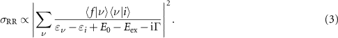
Todescato et al used the ratio between the LO and SO modes of CdSe and CdS to characterise the response of the nanostructure to shell growth and the concomitantly induced lattice strain [33]. In CdSe/CdS nanocrystals, grown using the single ion layer adsorption and reaction (SILAR) method, the CdSe SO mode increased strongly in intensity, relative to the LO mode, as the CdS shell thickness was increased, saturating at approximately 3 monolayers (∼ nm) (see figures 2 (A)–(C)). At the same time, the ratio between the CdSe and CdS LO modes indicated the increase in volume of the CdS shell. (The ratio of the integrated, fundamental LO peaks of a heterostructure can be used as a measure their chemical concentrations. This is particularly accurate for CdSe and CdS, because these semiconductors have similar ionicities and electronic dipole coupling constants [41].) If, instead of pure CdS, an alloyed CdZnS shell was grown from pre-mixed precursors, no significant change of the CdSe SO/LO ratio was observed up to 5 monolayers of CdZnS (see figures 2(D)–(F)). The different resonant Raman signals were interpreted as the strain-induced formation of an interfacial CdSex
S
nm) (see figures 2 (A)–(C)). At the same time, the ratio between the CdSe and CdS LO modes indicated the increase in volume of the CdS shell. (The ratio of the integrated, fundamental LO peaks of a heterostructure can be used as a measure their chemical concentrations. This is particularly accurate for CdSe and CdS, because these semiconductors have similar ionicities and electronic dipole coupling constants [41].) If, instead of pure CdS, an alloyed CdZnS shell was grown from pre-mixed precursors, no significant change of the CdSe SO/LO ratio was observed up to 5 monolayers of CdZnS (see figures 2(D)–(F)). The different resonant Raman signals were interpreted as the strain-induced formation of an interfacial CdSex
S alloy in response to the lattice mismatch between CdSe and CdS, while the alloyed CdZnS shell would retain the sharp interface due to its variable lattice constant. Tschirner et al observed a similar behaviour for CdSe/CdS particles with 5 CdS monolayers, which required an additional, third Lorentzian between the LO and SO peak for a consistent fit of the data. They also findings to alloying at the core/shell interface.
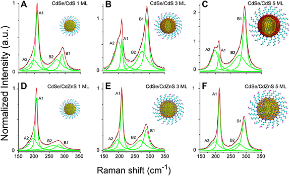
Figure 2. Surface-enhanced resonant Raman spectra of CdSe/CdS (A)–(C) and CdSe/CdZnS (D)–(F) core/shell nanocrystals with different shell thicknesses in monolayers (ML). The spectra consist of CdS-like phonon modes at ∼290 cm−1 (B1, B2) and CdSe-based modes centred at ∼209 cm−1 (A1, A2) to which the spectra are normalised. As the CdS shell thickness increases, the ratio of CdSe LO1 (A1-band) to SO1 (A2-band) phonons decreases, which points to an increasing influence of CdSeS alloy formation. No such behaviour is seen for CdSe/CdZnS particles. Reprinted with permission from [33]. Copyright (2013) American Chemical Society.
Download figure:
Standard image High-resolution imageIn addition to the SO phonon at the low frequency side, Dzhagan et al observed a high-frequency shoulder (HFS) to the LO phonon peak of CdSe and CdTe [42, 43], which has also been confirmed by others [44–46]. This feature is replicated in the overtones and decreases with increasing particle size, as well as the addition of a thick ZnS shell. The HFS has been attributed to either simultaneous scattering of optical and acoustic phonons or, again, to surface vibrations. Variations of the spectral shape and additional features to the bulk phonon mode are therefore useful, empirical probes for nanocrystal surface chemistry.
4. Excited state localisation and gradient formation
The attribution of the SO phonon to a pure surface mode has been contested: Kelley and co-workers demonstrated that the relative intensity of the SO mode increases if resonant excitation occurs into higher-lying excitonic states [47]. Based on atomistic, empirical force field calculations they determined that the LO mode was, indeed, based on displacement of atoms in the interior of the particle, while the vibrations of the SO mode involved all atoms, interior and surface. Rather than being a pure surface mode, the SO phonon appears to stem from a manifold of modes that are excited via EPC with the spatially more delocalised, higher excitons. These observations put the earlier assignments of the SO phonon as an indicator of possible phase mixing into perspective. The fact that the CdSe SO phonon intensity is sensitive to the growth of CdS, but not to that of the larger band gap materials CdZnS and ZnS [44, 47], points to the exciton delocalisation as the cause for the resonant excitation. Additionally, the possible formation of a CdSex
S over a Cdx
Zn
over a Cdx
Zn Se alloy, as suggested by Todescato et al, is in stark contrast to the facile cation diffusion discussed in the literature as a major contributor in the formation of graded shells [46, 48–50].
The fact that resonance Raman enhancement in nanocrystals depends on the spatial overlap of the exciton with the lattice in which the phonons propagate can be employed to map the exciton onto the atomic structure as a function of excitation energy. Lin et al performed resonant Raman experiments on CdSe/CdS nanostructures using a laser wavelength above the CdS band gap, so that the excitons delocalised into the shell material. They observed a strong dependence of the  ratio on size and shape of the CdS shell [51]. In spherical giant shell particles the intensity of the overtones increased up to a shell thickness of 2–3 nm. In anisotropic dot-in-rod particles the ratio was smaller, due to the smaller volume of the CdS shell that is accessible by the exciton spilling out of the CdSe core, only along the c-axis of the wurtzite structure. The
  ratio, which relates to the Huang-Rhys factor, and, hence, the polarisability of the material under RR conditions, is therefore proportional to the volume in which the exciton is localised.
Apart from the scattering intensity, Lin et al observed that the phonon lines also shift in energy as a function of the excitation wavelength under resonant conditions [29]. In CdSe/CdS particles the CdSe LO phonon shifted by 3–4 cm−1, while the CdS LO phonon varied by as much as 15 cm−1 as the resonance moved to increasingly hotter excitons above the band gap (see figure 3). The authors proposed the existence of multiple phonon modes, each found at a specific, radial position in the spherical particle, due to the lattice distortion at the interface. This follows the argument that higher excitation leads to a more delocalised excitonic state, which exhibits stronger EPC with phonon modes of the shell. However, the relative loss of intensity for the CdSe LO phonon does not agree with the localisation of the hole wave function in the particle core, as would be predicted by the effective mass approximation. It points to a more complex charge distribution for hot excitons, beyond the predictive capabilities of a continuum model that assumes parabolic bands.
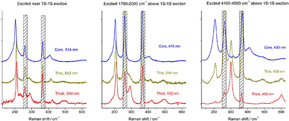
Figure 3. Resonant Raman spectra of base CdSe nanocrystals (blue) and CdSe/CdS core/shell particles with 0.5 nm (yellow) and 1.6 nm (red) thick shells. From left to right the excitation laser is shifted up in energy from the band edge exciton. As a result, the phonon lines were found to shift by as much as 15 cm−1. The relative intensities of the CdSe and CdS LO phonon lines are a measure for the spatial overlap of the exciton with the respective materials. The hatched bars cover two chloroform solvent lines. Reprinted with permission from [29]. Copyright (2015) American Chemical Society.
Download figure:
Standard image High-resolution imageThis observation by Lin et al underlines a fundamental issue that is at the core of many, sometimes contradictory reports: for RR to take place, the excitation laser must match a specific transition according to equation (3). Nearly all state-of-the-art nanocrystal samples have a size distribution, which translates directly to a variation of energy levels. The resonant Raman spectrum may therefore only represent a subset of the particles in the sample. In heterostructures, the selectivity becomes even more pronounced with a much larger number of parameters that affect the energy levels, such as core size, shell thickness and anisotropy, and gradient formation. A single wavelength experiment is therefore likely plagued by irreproducibility issues if the sample is changed.
Recently, we have employed Raman spectroscopy for the quantification of gradient formation between a ZnSe core and a CdS shell, in which both cations and anions can possibly diffuse across the core/shell interface [46]. In these experiments a 785 nm excitation laser was used, well below the band gap of the material. Any resonance Raman signal, characterised by strong overtones, must therefore stem from optically active mid-gap states. Hence, RR is a useful tool to correlate the spatial distribution and the energy levels of trap states, in addition to delocalised excitonic states. In the case of the graded ZnSe/CdS particles, strong LO phonons of CdSe and (with lower intensity) ZnSe were observed, but a very low CdS LO phonon peak (see figure 4). The CdS shell has a 4 to 8-fold higher volume than the core, so these spectra show unambiguously that (i) a strong cation exchange occurs across the core/shell interface during shell growth, leading to the CdSe signal, and (ii) that the excitons get trapped inside the core or at the core/shell interface. Increasing the shell growth temperature from 260 ∘C to 290 ∘C led to a stronger CdSe LO phonon and a 4-fold increased ratio of the first overtone to its fundamental mode,  , pointing toward an increased resonant enhancement, brought on by the phase mixing between core and shell.

Figure 4. Resonant Raman spectrum of graded ZnSe/CdS core/shell nanocrystals, synthesised at two different temperatures. The excitation occurred at 785 nm below the band gap into mid-gap states. The near-absence of a CdS-like peak (yellow ellipse) shows that the exciton does not delocalise into the shell. The relative intensity of the CdSe-like and ZnSe-like LO phonons indicate the degree of cation migration to and from the core. The increase of the 2LO1 phonon peak (green shade) at higher synthesis temperature is a measure of the increased EPC. Reprinted with permission from [46]. Copyright (2020) American Chemical Society.
Download figure:
Standard image High-resolution imageOur data adds to the body of work that makes mixing of the anion sublattice unlikely at reaction temperatures that keep the overall particle shape and structure intact [46]. There was no indication of the formation of a quaternary Znx
Cd Sey
S
Sey
S alloy due to anion migration at the core/shell interface, beyond the one monolayer contact of a sharp interface. The composition of ternary and quaternary phases can be determined from the phonon energies in the Raman spectrum, which shift systematically from those of the binary compounds. This has been mapped extensively by Zahn and co-workers [52, 53]. The Raman spectra of ternary alloys can exhibit either a one-mode or a two-mode behaviour, in which, respectively, either a single phonon mode appears following Vegard's rule, or two modes at wavenumbers similar to the constituent, binary compounds. A mixed-mode behaviour exists as well, in which the material switches between one and two modes as the molar fraction changes. The different behaviours are most successfully explained by the modified random-element isodisplacement (MREI) model by Chang and Mitra [54], which predicts two-mode behaviour if in an alloy Ax
B
alloy due to anion migration at the core/shell interface, beyond the one monolayer contact of a sharp interface. The composition of ternary and quaternary phases can be determined from the phonon energies in the Raman spectrum, which shift systematically from those of the binary compounds. This has been mapped extensively by Zahn and co-workers [52, 53]. The Raman spectra of ternary alloys can exhibit either a one-mode or a two-mode behaviour, in which, respectively, either a single phonon mode appears following Vegard's rule, or two modes at wavenumbers similar to the constituent, binary compounds. A mixed-mode behaviour exists as well, in which the material switches between one and two modes as the molar fraction changes. The different behaviours are most successfully explained by the modified random-element isodisplacement (MREI) model by Chang and Mitra [54], which predicts two-mode behaviour if in an alloy Ax
B C the atomic mass of one constituent MA
is smaller than the reduced mass µBC
of the binary material BC,
C the atomic mass of one constituent MA
is smaller than the reduced mass µBC
of the binary material BC,  with
with  . The behaviour of quaternary alloys is an extension of this principle: two modes are typically observed for mixtures Ax
B
. The behaviour of quaternary alloys is an extension of this principle: two modes are typically observed for mixtures Ax
B Cy
D
Cy
D of two cations and two anions, while compositions A
 Bx
Cy
D with either three cations or three anions tend to exhibit the three-mode (multimode) behaviour.
Bx
Cy
D with either three cations or three anions tend to exhibit the three-mode (multimode) behaviour.
Despite the lack of consensus on the origins of the observed phonons, Raman spectroscopy already allows for far-reaching predictions, based on empirical data. Mukherjee et al have published the most comprehensive study yet to correlate the structure of CdSe/CdS nanocrystals with the Raman spectral signature using multivariate fitting methods [41]. They included core/shell, core/gradient, and alloy compositions in their study as functions of particle size and S/Se ratio. Seven Lorentzians were used to fit the fundamental phonon modes (TO, SO, LO, and an additional mode attributed to surface effects or acoustic phonons), plus 10 more Lorentzians to fit the second harmonics. These assignments, with each peak yielding a frequency ωi , width γi and amplitude αi , were used in a multiple linear regression to a structural model, first assigning a core model (CdSe, CdS or alloy), and then a shell configuration (binary, alloy, gradient). The fit weighted each parameter (ωi , γi , αi ), which allowed to correctly assign the experimental spectra to the respective structural class. Furthermore, the structural assignment correlated well with predictions about the fluorescence quantum yield from effective mass approximations, which was higher if the shell was thicker and the interface more abrupt (see figure 5).

Figure 5. Chemometric analysis of the internal structure of CdSe/CdS and CdS/CdSe nanocrystals, fabricated via the SILAR method. The Raman spectrum (a) was fit to 17 Lorentzians with 4 parameters per function (b). Multiple linear regression (MLR) was employed to predict first a core model (c) and, in a second step, a shell model ((d)–(g)), which allowed to correctly classify the structures and identify core/shell (c), gradients (g), and homogeneous alloys (a). The simulated spectra in (c), (d) and (f) show the average spectrum as black curves. The most important contributions to the structure classification are shown as grey, shaded curves, and also given numerically below the spectra. Reprinted with permission from [41]. Copyright (2016) American Chemical Society.
Download figure:
Standard image High-resolution imageThe phonon modes did not all contribute to the structural model with the same weight. Rather, a few modes dominated the predictions: the area of the SO peak and width of the LO
 peak for the cores, and significant contributions of the second harmonics for the shell. In no case were the fundamental LO phonon lines of the core material a feature that contributed strongly to distinguishing the models. The authors expect the model to be applicable to other ternary nanomaterials that exhibit two-mode behaviour.
These findings combined show the power of Raman spectroscopy to extract structural information on the nanoscale, but emphasise the importance of Raman excitation profile experiments for semiconducting materials with quantised states above the band gap. One recent development that paves the way towards a more complete picture is the rapid acquisition of 2-dimensional Raman excitation maps as a function of both the excitation wavelength and Raman shift by Finnie and co-workers [55]. The method has so far only been applied to carbon nanostructures, but promises fast (∼ms to ∼100 s) acquisition of the 2D data matrices, owing to excitation with a supercontinuum laser and detection using a CMOS camera.
5. Time-resolved methods
Despite observing lattice vibrations in the 3–30 THz range, excitation via visible light allows for experiments with high time (50–200 fs) and energy (10 cm−1) resolution, as realised in femtosecond stimulated Raman spectroscopy (FSRS) [56, 57]. Herein, analogous to the probe pulse of UV/vis transient absorption spectroscopy, a sample is optically pumped by an actinic pulse into the nth vibrational level of an electronic, excited state. This state evolves as the density operator component  . The excitation is followed by a 20 fs probe pulse at frequency ωP
, which is overlapped with a 3 ps Raman pulse at ωR
(see figure 6(A)). The long Raman pulse provides the electric field that both excites the system into a higher, virtual state and couples with that state for the emission of the scattered photon. During the Raman pulse, the much shorter probe pulse interacts with the
. The excitation is followed by a 20 fs probe pulse at frequency ωP
, which is overlapped with a 3 ps Raman pulse at ωR
(see figure 6(A)). The long Raman pulse provides the electric field that both excites the system into a higher, virtual state and couples with that state for the emission of the scattered photon. During the Raman pulse, the much shorter probe pulse interacts with the  operator and creates a coherence
  with a second vibrational state
  , i.e. it puts the system in a superposition of both states. This superposition state oscillates between the two possible states with a frequency ω0 and decays with the dephasing time
  on the timescale of picoseconds. It is the frequency of this coherence that determines the position of the Stokes and anti-Stokes Raman peaks at
  .
.
Figure 6. (A) Experimental setup of the 3 pulse FSRS experiment. (B) FSRS spectrum of CdSe nanocrystals showing the Rayleigh, Stokes and anti-Stokes signals on top of the probe pulse background (black) and after background subtraction (red). (C) Recovery of the stimulated Raman signal of the CdSe LO phonon for different actinic pump intensities or average number of excitons per particle  . (D) Schematic of the biexciton cooling in CdSe nanocrystals. The emission of phonons and, consequently, stimulated Raman scattering, is indicated. Reprinted with permission from [61]. Copyright (2018) American Chemical Society.
Download figure:
Standard image High-resolution image
At first glance, the method appears to circumvent Heisenberg's Uncertainty Principle by giving both a high temporal and spectral resolution. The narrow probe pulse yields a defined time point at which the coherence is created, yet its width does not limit the spectral resolution, because the scattered photons can be emitted as long as coherence exists in the presence of the E-field of the Raman pulse. The spectral resolution (10–20 cm−1) is therefore determined by the convolution of the temporal width of the Raman pulse and the dephasing time of the coherence. However, the spectral width of the probe pulse ensures the detection of all Raman-active transitions simultaneously. The Raman spectrum appears on a background of the probe pulse envelope centred at ωP (see figure 6(B)). For semiconductor nanocrystals, FSRS brings another advantage as fluorescence is not detected in the direction of the stimulated Raman signal, circumventing the issue that affects RR spectroscopy.
The delay between the actinic and probe pulse is systematically varied to probe the evolution of the system across the potential energy landscape. Hence, FSRS is a powerful technique to investigate ultrafast processes of the atomic backbone of a material under excitation. It has first been applied to probe intra-band relaxation of hot carriers in semiconductor nanocrystals in 2013 by Hannah et al [38]. The stimulated Raman scattering intensity in these nanocrystals is proportional to the exponential of the inverse LO phonon occupation number. Phonons are bosons and obey the Bose–Einstein statistics. Therefore, the presence of phonons in a hot nanocrystal reduces the probability of further phonon generation through stimulated Raman scattering. This is observed as a depletion of the Stokes and anti-Stokes Raman signals in the sub-picosecond timescale, as the hot excitons created by the actinic pulse cool via LO phonon scattering. The FSRS signal recovers on the order of  –2 ps as the LO phonons further decay into acoustic phonons. This fast recovery is followed by two slower recovery processes,
  –30 ps and
  –230 ps, which have been attributed to the formation of a quasi-equilibrium between optical and acoustic phonons. The thermal energy is finally dissipated to the organic surface ligands and solvent molecules. Comparison of the phonon generation rates with transient absorption measurements showed consistent time constants with hole relaxation, making this the most likely, dominant mechanism for the emission of LO phonons. The absence of a significant size dependence of the Raman gain supports cooling of the more strongly quantised electrons via Auger excitation of the holes instead of direct phonon emission, as has been proposed in the literature [58–60].
A follow-up study by Harvey et al investigated the dependence of the FSRS signal on the pump fluence of the actinic pulse [61]. A higher fluence excites a population of biexcitons and multiexcitons in the nanocrystals, which decay via an Auger-mediated relaxation pathway that leads to a repeated intra-band hole excitation/cooling and emission of LO phonons. The experiments showed a complete disappearance of the Stokes and anti-Stokes scattering signals at high pump intensity, supporting large phonon populations. The FSRS signal recovery was markedly slower than after excitation of single excitons. The longer lifetime of the phonon population was attributed to the stronger heating of the nanocrystal lattice, which shifts the equilibrium between the optical and acoustic modes further to the higher energy optical phonons. Hence, the LO phonon population dissipates more slowly through an acoustic phonon bottleneck, which is the only way of transferring heat out of the nanocrystal (see figures 6(C) and (D)).
A different method to probe lattice vibrations in a time-resolved manner is coherent anti-Stokes Raman scattering (CARS). In this experiment, a pump pulse with frequency ωp
is used to promote the sample into a virtual state, which is again a linear combination of eigenstates. By itself, the virtual state would quickly evolve back to the ground state and scatter the excitation light. In CARS the pump beam coincides with a second Stokes beam with frequency ωS
so that the difference in frequency between the two beams,  corresponds to the transition from the ground state into a vibrational state. The nonlinear interaction of the two beams efficiently produces a coherent superposition of the ground and vibrational states. A third probe pulse, again with the frequency ωp
, can now return the superposition back to the ground state, upon which a photon with the frequency
corresponds to the transition from the ground state into a vibrational state. The nonlinear interaction of the two beams efficiently produces a coherent superposition of the ground and vibrational states. A third probe pulse, again with the frequency ωp
, can now return the superposition back to the ground state, upon which a photon with the frequency  of the anti-Stokes line is emittied. A time delay τ between the first two pulses and the probe pulse allows to probe the time-dependence of the coherence. The direction of the scattered beam is defined by the wave vectors
  and can thus be separated from the excitation pulses. As it appears at a higher energy than the Rayleigh scattering, the anti-Stokes signal has the benefit of not overlapping with a fluorescence signal.
Reports on the application of CARS on semiconductor nanocrystals are scarce. Waltner et al have observed a strongly reduced dephasing time of 0.9 ps in CdSex
S embedded in a glass matrix at T < 10 K, compared to bulk semiconductores (5–9 ps) [62]. This was attributed to energy dissipation to either the particle surface or the surrounding matrix. The central issue with this method was that the CARS signal was swamped by a degenerate four-wave mixing signal. It is caused by the spectral overlap of pump and Stokes pulse, which have a broad spectral bandwidth due to the femtosecond pulse duration required to achieve the temporal resolution.
6. Conclusions
In conclusion, different variants of Raman spectroscopy have been applied to investigate several fundamental aspects of semiconductor nanocrystals. These encompass the verification of the structural similarity to bulk crystals, quantification of lattice strain, the formation of solid solutions at heterointerfaces, and the spatial distribution of excitonic states. Even further insights have been gained by applying time-resolved methods, in particular femtosecond stimulated Raman scattering (FSRS), which yields detailed information on the energy dissipation of hot carriers. While Raman spectroscopy has proven to be an extremely useful and crucial tool for fundamental questions regarding the structure and dynamics of nanoscale semiconductors, it has by no means become a routine method. Apart from the technical complexity and costs of the more advanced methods, this is mainly due to two issues: there is not yet a consensus on the cause for some of the Raman signals observed in nanocrystals, the SO phonon and the HFS. Also, the need to excite resonantly via EPC causes reproducibility issues with samples that exhibit both a size distribution and a size-dependence of its energy levels of the confined exciton. Recent advances in the development of faster and more reliable light sources and spectrometers are promising developments that will see Raman spectroscopy applied more routinely in the characterisation of nanomaterials.
Acknowledgments
The author is grateful for support by the Zukunftskolleg Konstanz through a 5-Year Marie Curie Research Fellowship and by the Fonds der Chemischen Industrie (FCI) through a Liebig Fellowship.
Data availability statement
No new data were created or analysed in this study.