

Abstract
We discuss the benefits and showcase the applications of using a fast, hybrid-pixel detector (HPD) for 4D-STEM experiments and emphasize that in diffraction imaging the structure of molecular nano-crystallites in organic solar cell thin films with a dose-efficient modality 4D-scanning confocal electron diffraction (4D-SCED). With 4D-SCED, spot diffraction patterns form from an interaction area of a few nm while the electron beam rasters over the sample, resulting in high dose effectiveness yet highly demanding on the detector in frame speed, sensitivity, and single-pixel count rate. We compare the datasets acquired with 4D-SCED using a fast HPD with those using state-of-the-art complementary metal-oxide-semiconductor (CMOS) cameras to map the in-plane orientation of π-stacking nano-crystallites of small molecule DRCN5T in a blend of DRCN5T: PC71BM after solvent vapor annealing. The high-speed CMOS camera, using a scintillator optimized for low doses, showed impressive results for electron sensitivity and low noise. However, the limited speed restricted practical experimental conditions and caused unintended damage to small and weak nano-crystallites. The fast HPD, with a speed three orders of magnitude higher, allows a much higher probe current yet a lower total dose on the sample, and more scan points cover a large field of view in less time. A lot more faint diffraction signals that correspond to just a few electron events are detected. The improved performance of direct electron detectors opens more possibilities to enhance the characterization of beam-sensitive materials using 4D-STEM techniques.
Export citation and abstract BibTeX RIS

Original content from this work may be used under the terms of the Creative Commons Attribution 4.0 license. Any further distribution of this work must maintain attribution to the author(s) and the title of the work, journal citation and DOI.
1. Introduction
1.1. 4D-STEM experiments for materials characterization
Materials characterization using transmission electron microscopy (TEM) has evolved rapidly over the last decade thanks to improvements in instrumentation technologies, particularly with the development of direct electron detectors (DEDs). Compared to conventional scintillator coupled detectors (either using charge-coupled devices or complementary metal-oxide-semiconductor (CMOS)), DEDs avoided conversion processes, thus eliminating sources of noise and loss of signal due to electron-to-photon conversion in a scintillator, and photon transfer through a fiber-optic coupling. The speed at which signals are read out in DEDs has been improved drastically. Furthermore, electron counting significantly improved the detection quantum efficiency (DQE) to almost unity at zero frequency and modulation transfer function [1, 2], which is an important characteristic of a detector to record fine details. All these factors have led to the great success of TEM imaging of biological structures in the field of Cryo-EM [3, 4] and beam-sensitive materials [5, 6].
The increased speed of DEDs led to renewed interest in diffraction experiments using Scanning TEM (STEM) approaches, commonly referred to as 4D-STEM [7]. A 4D-STEM experiment can be briefly described as scanning the electron beam over the sample in an array while collecting the electron scattering (diffraction) pattern at every point with a pixelated detector. The resulting (2D) array of (2D) diffraction patterns (DPs) (i.e. 4-dimensional datasets) contains a wealth of structural information from the studied sample. Its analysis can result in flexible imaging modalities with virtual STEM detectors, in a comprehensive analysis of crystalline phases, orientation [8, 9], strain state [10, 11], and ultimate spatial resolution and high contrast with ptychography reconstruction approaches [12, 13]. We note that the efficiency of information transfer in 4D-STEM experiments is highly dependent on the sample and experimental conditions, in particular, the convergence angle and diffraction space sampling [9, 14–17]. Experimental parameters, therefore, need to match each application case, and structural information out of 4D-STEM datasets usually needs to be extracted with appropriate post-acquisition algorithms, from using simple virtual apertures, and Bragg peak analysis [9], to momentum space weighting like first- or second-moment measurements [18, 19] to more complex inverse problem solving including multi-slice ptychography [12, 20]. Figure 1 illustrates examples of such 4D-STEM application cases that we have recently studied, ranging from momentum-resolved STEM imaging for revealing heavy and light elements simultaneously, to studying vacancies in 2D oxides with multi-slice ptychography reconstruction, to nano-crystalline thin film orientation mapping. In each case, the convergence angle, sampling in real space and reciprocal space, as well as the total dose had to be adjusted so that the information of interest could be efficiently transferred and extracted. In consonance with the shift from conventional TEM to STEM imaging in the field of materials characterization over the last decade, 4D-STEM represents one of the current frontiers in characterization of materials using electron microscope due to the recent and increasing availability of suitable electron detectors.

Figure 1. Examples of fast 4D-STEM results in three different application fields, from (a) momentum-resolved STEM imaging to (b) ptychography to (c) phase and orientation mapping of nano-materials. Typical raw diffraction patterns and histogram with counts of the diffraction pattern are shown to the right of each evaluated data image. (a) A first-moment image of SmB6 [110], obtained by evaluating the center-of-mass shift in the diffraction pattern, revealing heavy Sm and light B atomic columns. Data were acquired using a 30 pA electron probe; pixel dwell time of 10 µs; a full detector area at bin2, i.e. with data dimensions of 1000 × 1000 (real space) and 96 × 96 (diffraction); and a 10 s acquisition time. (b) A ptychographic reconstructed (using a multi-slice algorithm [20]) phase image of Gd2O3 nano-crystals with oxygen vacancies revealed (arrow). Data were acquired using a ∼150 pA probe; pixel dwell time of 10 µs; data dimensions of 256 × 256 × 96 × 96; and 0.7 s acquisition time. (c) X-axis (left half) and z-axis (right half) orientation maps of a polycrystalline, [111] textured gold thin film, as analyzed with automated crystal orientation mapping [9] method. Data was acquired using a ∼65 pA probe, pixel dwell time of 50 µs, data dimensions 400 × 400 × 192 × 192, and 8 s acquisition time.
Download figure:
Standard image High-resolution image1.2. Using hybrid pixel detector (HPD) for 4D-STEM
The acquisition of 4D-STEM datasets imposes a few challenging requirements on the electron detector. First, a high frame rate is desirable so that the 4D-STEM collection can be performed at a high speed. Besides the immediate impact on the sample area coverage and measurement sampling, a fast scanning speed applied to (4D)-STEM measurement reduces the effects due to sample drift and provides additional flexibility for electron dose management in the context of decreasing sample damage. Ideally, a 4D-STEM setup with an acquisition time similar to that of conventional STEM imaging is desirable, so that the same experimental considerations are applicable. The examples in figures 1(a) and (b) were recorded with a pixel time of 10 µs to allow for minimal sample drift, and figure 1(c) was recorded with a total frame acquisition time of 8 s to achieve the necessary yield in terms of real space region of interest coverage and reciprocal space sampling (i.e. speed vs. number of detection pixels).
For the second requirement, high sensitivity to counting single electron hits with minimum readout noise is desirable for recording electron scattering at moderate to low doses and fast frame rates. With typical STEM beam currents ranging from 100 pA to less than 1 pA, short acquisition times (10 µs) per scanning pixel yield approximately 6000 to less than 60 electron counts per detector frame. Depending on the applications, these hits can be spread over many detector pixels, as in the cases of momentum-resolved STEM (figure 1(a)) and ptychography (figure 1(b)), it is expected that a significant portion of the DP outside the bright field (BF) disk will discriminate between single electrons and no events, as is obvious when examining the histograms with counts.
Third, a high electron count rate or, equivalently, a high dynamic range is desirable to account for localized intensities originating from the BF disk or diffraction spots at strong diffraction conditions (cf. Figure 1(c)). Depending on the camera length setup and the sample's crystalline structure, a few detector pixels may receive most of the transmitted and/or diffracted electron signals and possibly saturate or incur damage. For instance, 4D-STEM experiments aim for nanoscale structure phase and orientation studies, similar to that shown in figure 1(c), and these can reach a localized and instantaneous beam current over 1 pA per detector pixel, equivalent to ∼107 electrons per second. An electron detector that can sustain a high count rate per pixel with a linear output and is not susceptible to beam damage with repeated exposure to high electron fluxes is necessary for flexible 4D-STEM experiments.
A few technologies allow for the direct detection of electrons, including p-n junctions (pnCCD) [21], monolithic active pixel sensors (MAPSs) [22], and HPDs [23]. Considering the range of 4D-STEM experiments and the detector requirements, especially the fast frame rate and the extended dynamic range, the HPD concept is particularly attractive. Here, we briefly summarize the character of HPDs and refer the readers to more comprehensive reviews, e.g. [1, 2] for a more detailed overview of detector technologies.
Initially developed to address x-ray detection with a high dynamic range, the HPD concept combines a sensor material and an application-specific integrated circuit (ASIC) fine-tuned to the detection context. Its working principle [24] involves the complete absorption of the incoming electron energy at the sensor, which is most commonly a thick slab of Si or CdTe. This process generates multiple electron-hole pairs at the sensor, which are then separated by an electrical bias applied between the ASIC and the sensor layers. The individual ASICs at every detector pixel collect the signal originating from the charge carriers through bump bond connections and independently amplify and compare it against a threshold, which defines the electron counting and nullifies noise contributions from the electronic circuit. Each ASIC unit includes fast-switching counters to register incoming electron counts continuously with minimal dead time (100 ns).
A limitation of the HPD concept for such a design approach is the limited number of pixels. Large pixels are necessary to both contain the electron-hole pairs generated in the sensor by incoming high-energy electrons with energies up to 300 kV and the necessary ASIC circuitry for fast electron counting at each pixel position. Current HPDs optimized for electron detection have pixel sizes ranging from 55 to 150 µm, restricting total (single chip) array sizes to 128 × 128 (e.g. EMPAD from Thermo Fisher) to 256 × 256 (e.g. Medipix3). Tiling multiple sensor chips, or multiple ASICs sharing a larger piece of sensor could result in a larger footprint and more pixels, e.g. 512 × 512 (quad Medipix3 or QUADRO from DECTRIS) and 1028 × 1062 (SINGLA from DECTRIS), however at cost of compromised speed due to reduced space for readout channels in every single chip. With the total size constraint to remain TEM-compatible, HPDs pixel number is not generally well suited for TEM imaging experiments compared to MAPS counterparts, which can surpass 4096 × 4096 pixels with down to 5 µm pixel size.
In contrast, HPDs excel in electron diffraction applications, 4D-STEM, and electron energy-loss spectroscopy experiments, as these prioritize sensitivity and dynamic range [25]. The most recent HPDs [26] can simultaneously provide sensitivity to single electron events, counting capability up to 10 pA beam current per detector pixel, and frame times below 10 µs. This performance allows fast 4D-STEM experiments suited to study beam-sensitive samples [27] and even in situ observations.
The most common readout architecture in current DEDs is frame-based, where the electron hit events registered in all detector pixels (either with or without counting) for a defined period are read out once as a 'frame'. In fast 4D-STEM experiments with moderate to low doses and electron counting, the signals can be very sparse (cf histograms in figures 1(a)–(c)). Read, transfer, and storage of sparse data in a frame-based manner is very inefficient. The event-based architecture of readout, originally driven by applications in motion detection [28], has recently been made available for electron detection (coupled to either HPD [29] or MAPS [30]) in the TEM. In such a detector, single electron hits are registered by their location and time, forming a data stream of events. The interval of electron hit events could reach less than a couple of nanoseconds [31], making these detectors shine in cutting-edge applications such as coincidence spectroscopy [29, 31, 32] and the study of ultrafast phenomena [33]. For 4D-STEM applications, researchers have shown pixel dwell time down to ∼100 ns [29], thus a nominal frame speed of up to 10 MHz could be reached. However, the exposure rate was limited to approximately 40 × 106 electrons per second across the whole sensor, equivalent to just over 600 e−/pixel/s (or 0.1 fA per pixel). This limitation is due to the electron count rate the ASIC can process, as each event has to be transferred over a communication channel (with limited bandwidth) towards a field programmable gate array (FPGA) that takes care of repackaging and grouping the data and sending it over another communication channel towards further processing or storage. This suggests that frame-based detectors currently retain an advantage for imaging intense features such as the bright-field or strong diffraction disks in 4D-STEM.
In 4D-STEM applications, the number of detector pixels determines the reciprocal space sampling. While it is not as critical as in imaging applications, e.g. cryo-EM, and superb resolution have been demonstrated in ptychography using only 128 × 128 pixels [12] or less [34], a sufficient number of pixels is still preferred for crystallography-related studies where accurate location and intensity of Bragg peaks are critical. Although Bragg peaks/disks are usually very intense at moderate dose conditions (e.g. in figure 1(c)), they might hide in shot noise (even while using DEDs with a DQE close to unity) at extremely low dose conditions if beam disks cover a range of pixels. This can be even worse when the sparse background of diffuse scattering presents, lowering the (diffraction) signal to background ratio. In such an extreme scenario, one has to balance signal detectability and reciprocal space sampling, and further strategies might be needed to help enhance the detectability of diffraction signals both in data acquisition and algorithm in post-processing.
1.3. Dose-efficient diffraction imaging of nano-crystalline structures in soft materials
A significant proportion of functional nanomaterials presents high susceptibility to structural damage when exposed to a high-energy electron beam, which makes them very challenging to characterize at high spatial resolution using TEM. Remarkable examples in Material Sciences applications are Zeolites [35], MOFs [36], and polymeric and organic structures [16, 37–39], which have importance in fields ranging from catalysis and gas separation to organic electronics and organic solar cells (OSC).
Direct observation of organic molecular nanocrystals using electron microscopy is extremely challenging, particularly due to their radiation sensitivity and complex structure. Such crystals may only tolerate high-energy electron doses of up to a few e−/A2 before their structure gets damaged, which is orders of magnitude lower than the doses that are commonly used for TEM imaging of most inorganic materials. Electron diffraction experiments have distinctive advantages over imaging for structural characterization of dose-limited nanocrystals, as the crystallographic information is recorded as spot-like DPs. This leads to an increase in the signal-to-noise ratio (SNR) of the elastically diffracted electrons, as well as an improved diffraction signal-to-background ratio (SBR) to the inelastically scattered background. The latter is especially important for structural information of large unit cells in which diffraction spots are located at small diffraction angles. Electron crystallography methods [40, 41] are very capable to study the structure of beam-sensitive crystals (e.g. those used for pharmaceutical applications [42]), and information can be obtained from spatially averaged diffraction experiments, where the spatially resolved structure is of less importance. 4D-STEM experiments with small semi-convergence angles α (nano-beam diffraction or NBD) have recently demonstrated the retrieval of rich structural information from soft materials [39, 43, 44], including organic crystals with large unit cells and corresponding diffracted signals at small scattering angles and also analysis of amorphous materials [45]. Furthermore, we have recently introduced 4D-scanning confocal electron diffraction (4D-SCED) as another 4D-STEM modality that optimizes dose efficiency and angular resolution [16].
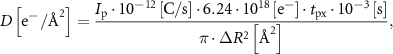
4D-SCED involves a defocused pencil-beam illumination at the sample plane, combined with a confocal electron optics setup and a pixelated detector that records the focused spot-like DPs (figure 2 left). The defocused illumination at the sample reduces the dose and generates a more homogenous electron beam-sample interaction compared to the interaction in a normal focused-beam NBD setup. At the same time, the confocal optics generates spot-like diffraction signals, boosting both the SNR and the SBR. This way, the spatial and angular resolution are largely decoupled from illumination convergence due to the newly introduced parameter defocus z. To balance both spatial and angular resolution and to achieve a more homogeneous beam-specimen interaction, a semi-convergence angle α on the order of ∼1 mrad and a large defocus (z≫ t) of a few micrometers are typically applied. The experiment optimization provided by 4D-SCED allows for the study of complex nano-crystalline structures of soft materials at few nm spatial resolution and enables the direct in situ observation of nanocrystals growth and coarsening in bulk heterojunction (BHJ) thin films [16, 46].
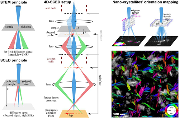
Figure 2. Nano-beam diffraction 4D-STEM and dose-efficient 4D-SCED setups (left), and the principle of orientation mapping the nano-crystallites in bulk heterojunction organic solar cells (right). Reproduced from [16]. CC BY 4.0.
Download figure:
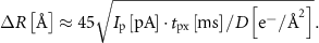
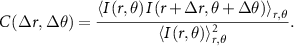
Standard image High-resolution imageThe principle of orientation mapping, as applied to the nano-crystallites in BHJ OSCs is schematically shown on the right side of figure 3. Typical π-stacking crystals used for OSCs form orthogonal or close to orthogonal unit cells [47]. Their lattice spacing of π-stacking (usually defined as b direction) is in the range of 3–4 Å, perpendicular to the in-plane lattices a and c with lattice spacing in the range of a few nanometers and characteristic Bragg angles smaller than 1 mrad considering the typical electron energies used for electron diffraction in a TEM. The identification of edge-on and face-on domains can be carried out from the spacing of their respective Bragg reflections, while their in-plane orientation can be determined from the in-plane angle of the Bragg peaks. Therefore 4D-STEM characterization allows us to unambiguously reveal the size and orientation of the nano-crystalline domains, which are critical for understanding and modeling the charge carrier transport properties [38], given that the observations faithfully represent the pristine materials' structure.

Figure 3. Comparisons of data acquired from the same BHJ sample using (a)-(e) an NBD 4D-STEM setup and (f)-(j) a 4D-SCED setup. Unprocessed, raw diffraction patterns from 2 × 2 scan pixels in each datasets corresponding to edge-on (b), (g) or face-on (d), (i) domains are extracted and shown. v-BF (a), (f) images are calculated using disk aperture around the transmission beam, and v-ADF images with radius range [2.35, 2.75] nm−1 corresponding to the edge-on domains (c), (h) and [0.49, 0.88] nm−1 corresponding to face-on domains (e), (j) are calculated with the annular apertures. Intensity line profiles extracted from (b), (g) and (d), (i) are shown in log scale in (k) and (l), respectively, for comparison.
Download figure:
Standard image High-resolution imageThe 4D-SCED setup is a particularly demanding diffraction experiment for detectors. Besides having most of the primary electron beam concentrated in the transmission spot covering few pixels, the diffracted components of interest can be very weak that contain just a few electron counts at the total electron dose allowed by the sample. The direct beam component presents reduced information and is mostly used as a reference point for evaluation of the diffracted components. While the hardware or software masking of this region may be helpful to adjust the experiment to the dynamic range of the electron detector, they prevent the correction of diffraction shifts across the field of view (FoV). This is particularly relevant if large areas are scanned, e.g. to obtain statistical information about the sample, as the scan and de-scan coils' imperfections become more evident and result in significant position-dependent diffraction shifts [16]. Therefore, recording the complete unmasked DP is necessary for effective post-processing of 4D-SCED datasets.
Seminal 4D-SCED experiments using conventional scintillator-mediated CMOS detectors were limited to low beam currents, usually below 5 pA, and slow acquisition speeds, typically up to 300 frames per second (fps) [16]. This was to conform both to the sample sensitivity to electron damage and the frame rate and dynamic range allowed by the detector technology, and it resulted in 4D-SCED datasets with a limited FoV. The recent availability of HPD technology for electron diffraction improved the experimental flexibility of dose-efficient 4D-SCED, as applied to diffraction imaging of molecular nano-crystalline structures. Here we demonstrate the figure of merit to evaluate such experiments and compare the performances of different detector technologies.
2. Method
BHJ thin films consisting of DRCN5T small molecules blended in PC71BM, and processed by solvent vapor annealing in a CS2 atmosphere for 720 s, were used as a reference sample in this study. An extended description of the sample preparation and comprehensive characterization has been reported in earlier studies [16, 46].
4D-STEM experiments (using both 4D-SCED and NBD setups) were performed on two TEMs: a thermo fisher scientific (TFS) Titan Themis3 equipped with a Ceta 16M and operated at 300 kV, and a TFS Spectra 200 equipped with a Ceta-S and a DECTRIS ARINA detector, operated at 200 kV. Experimental conditions for 4D-SCED were designed according to the previous study [16] to satisfy (1) both the instantaneous dose and the total dose stayed below the limited dose budget of 5 e− Å−2 measured before [16], and (2) that the BF spots did not saturate. Under such conditions, the spatial resolution is dose-limited, and thus sampling should match the spatial resolution. We can use the instantaneous dose at any probing point according to the following formula:
with an  probe current (in pA), a
  dwell time at each pixel (in ms) and the
  dose budget (in
  ) which can be evaluated from selection area electron diffraction (SAED) experiments as a function of dosage, to estimate the dose-limited spatial resolution
  in a scanning probe experiment,
For a given dose budget and detector speed, the resolution can be set by the probe current; however, a beam current that is too low will make experiments impractical. For example, on the Spectra platform using a Ceta-S camera with a dwell time of  , setting the probe current to
  , and the dose budget of
  , we expect a spatial resolution of
  . To achieve this condition, using the smallest convergence angle
  on the TEM, a defocus value of
  is required. In this way, we have chosen parameters for all three detectors; the full parameters are summarized in table 1. Before the experiments, the dose conditions are determined based on measured probe current and afterward evaluated based on calibrated detector counts from the acquired datasets. This will be discussed further in the next section. The flu-screen readings on both TEMs are calibrated using a Faraday cup. The lowest reading of the fluorescent screen on Titan is 30 pA with the smallest measurable increment of 1 pA and the lowest reading on Spectra is 1 pA and 1 pA increment. To reach currents below 30 pA on the Titan and below 1 pA on Spectra, we first inserted the largest condenser aperture and measured the screen current as a function of the monochromator or gun lens excitation. Then this function is scaled by a factor of 9 (i.e. the area ratio of the largest condenser aperture to the smallest) and extrapolated to the desired low currents. We refrained from using different spot sizes to keep the optics setting stable and consistent and reduce the complexity of aligning 4D-SCED. The effective camera length in 4D-SCED (set by image magnification using projection lenses) was set to keep the pair of π-stacking diffraction spots (∼2.6 nm−1) within about 60% of the detectors frame, leaving enough room to allow for the post-processing correction of diffraction shift due to scan imperfections at large FoVs.
Table 1. Dose calculation for 4D-SCED with different detectors and matching experimental conditions.
| Ceta 16M | Ceta-S | ARINA | |
|---|---|---|---|
| Frame rate (fps) | 25 | 280 | 100 000 |
| Detector pixels | 4096 × 4096 | 4096 × 4096 | 192 × 192 |
| Center 512 × 512 bin2 | Center 512 × 512 bin1 | Bin2 to 96 × 96 | |
| Pixel dwell time (ms) | 40 | 3.57 | 0.01 |
| 4D-SCED probe semi-convergence (mrad) | 0.7 | 0.85 | 0.85 |
| Defocus (µm) | 20 | 5 | 5 |
| Probe-sample interaction radius (nm) | 14 | 4.3 | 4.3 |
| Interaction area (nm2) | 615.8 | 14.5 | 14.5 |
| Probe current (pA) | 1 | 1 | 30 |
| Scan sampling (nm) | 35 | 8.8 | 4 |
| Scan size (pixels) | 80 × 80 | 250 × 250 | 1000 × 1000 |
| Scan frame time (s) | 256 | 223 | 10 |
| Frame area (nm2) | 7.84 × 10⁶ | 4.84 × 10⁶ | 1.60 × 10⁷ |
| Number of electrons per Coulomb (e− ) | 6.24 × 10¹⁸ | ||
| Electron flux (e− /s) | 6.24 × 10⁶
| 6.24 × 10⁶
| 1.87 × 10⁸
|
| Sum | 249 600 | 22 286 | 1872 |
| Dose per probe (e− /Å2) | 4.05 | 4.42 | 1.29 |
| Sum | 1.60 × 10⁹
| 1.60 × 10⁹
| 1.87 × 10⁹
|
| Dose per scan (e− / Å2) | 2.04 | 3.3 | 1.17 |
a This number is extrapolated (cf the Method section) from a calibrated flu-screen, which has a lowest possible reading of 30 pA. b These numbers are direct read from the calibrated flu-screen, which has a lowest possible reading of 1 pA with an increment of 1 pA. c These numbers are calculated using flu-screen reading, either extrapolated a or directly read b. d These numbers are calculated via intensity sum counts of an average single detector frame with the specified conversion factor of 7 counts/e− for Ceta 16M, 25 counts /e− for Ceta-S, and 1.65 counts/e− for Arina at threshold voltage of 17.5 kV.
The Ceta 16M camera is a scintillator-coupled CMOS device by TFS, mounted on a Titan Themis platform (without speed enhancement). It runs up to ∼75 fps using a center 1/8 sensor area (512 × 512) read out with high speed, rolling shutter, and continuous readout mode when controlled via Velox software, limited by the data bandwidth. For 4D-STEM experiments with probe synchronization via TIA software, however, it could reach a maximum frame rate of only 25 fps with a readout of 512 × 512 pixels. Inappropriate settings of the camera mode (e.g. high speed/high quality, enable/disable rolling shutter) and dwell time may lead to a significant portion (>50%) of dead time during which the electron dose is wasted. A dynamic range of about 13-bit (∼8 000 counts) can be reached on a single frame readout, which is equivalent to an approximate saturation level of ∼320 e− pixel−1 or ∼0.015 pA pixel−1 at the maximum frame rate and 300 kV electrons. Operating the camera in frame summing mode could reach much higher dynamic range but this slows down dramatically in 4D-STEM applications.
The Ceta-S camera is mounted on the TFS Spectra platform (with speed enhancement). It follows a similar concept similar to that of the Ceta 16M, however, it uses a scintillator optimized for lower electron doses and an improved data bandwidth that allows a maximum frame rate of 300 fps at 512 × 512 pixels when operated via Velox software for continuous recording and 280 fps for 4D-STEM experiments. So the dead time is estimated to be about 7%. A dynamic range of about 13-bit (∼8000 counts) can be reached on a single frame readout, which is equivalent to an approximate saturation level of ∼320 electrons per readout pixel or ∼0.015 pA per pixel at the maximum frame rate and 200 kV electrons. We note that the limited dynamic range that was observed in the acquired datasets was likely limited by the bandwidth of data transfer rather than by the physical scintillator or CMOS chip.
The DECTRIS ARINA is a fast HPD with 192 × 192 pixels mounted opposite to the Ceta-S camera position. In this work, we used the version with a CdZnTe sensor. A flat field reference was acquired before the experimental sessions and applied to correct the inhomogeneity of pixel response. It is operated with a USG external scan generator and 'EMplified' interfacing software by TVIPS, allowing 4D-STEM experiment synchronization up to a maximum frame rate of 120 000 fps at a 96 × 96 pixels readout. Even though the 12-bit dynamic range can be reached for single frames at the maximum readout speed, ARINA provides a linear electron count output of up to about 10 pA per pixel. The ARINA detector was run in 'slave' mode, and a constant dead time of 500 ns was set in 'EMplified' to safely accommodate the small mismatch in the tails of onset/offset triggers and the camera readout time. This resulted in about 5% dead time for the dwell times (10 µs) that were used in the experiments reported here.
The 4D-STEM datasets were imported and mostly processed with Gatan DigitalMicrograph and the correlation maps were obtained using the corresponding functions in py4DSTEM [9, 16, 48]. The Ceta 16M outputs are in a binary SER file format and the Ceta-S camera adopts an MRC file format [49], while the ARINA detector uses an open HDF5 format with lossless compression (LZ4 and bit shuffle [50]). For example, the 4D-STEM dataset represented in figure 3(c) which contains 106 DPs with 96 × 96 binned detector pixels each and 12-bit information depth has a total data size of 1.6 GBytes.
The analysis of π-stacking nano-crystallites relies on virtual dark field imaging method, which is highly efficient. The 2D orientation map of the edge-on crystal domains was obtained by directly evaluating the virtual dark-field images using sector apertures with a radius between 2.6 and 2.8 nm−1 and (in-plane) angular increment of n degrees. In this way, a total of 360/n dark-field images were calculated, and each image corresponds to an in-plane diffraction angle φ = ni defined by the sequence i of the virtual apertures. This reduces the 4D dataset to a 3D dark-field image stack. At any (real space) scanning pixels position (x, y), we search for the intensity maxima M along the dark-field image stack and mark their location as φ, which defines a 2D grid of complex numbers M(x, y)eiφ(x, y) (equivalent to 2D vectors). Finally, the 2D grids of complex numbers are visualized using a color wheel scheme as presented in figures 2 and 4.

Figure 4. Results of in-plane orientation mapping of π-stacking nano-crystallites of BHJ thin film sample with 4D-SCED. The color-coded orientation maps result from experiments using (a) a CMOS camera at 25 fps; (b) a low-dose optimized CMOS camera at 280 fps; (c) a fast HPD at 100 000 fps. Insets show example diffraction patterns extracted from the color dot marked positions from each dataset. (d–f) Intensity line profiles extracted from raw diffraction patterns from (a) to (c). (g–i) Spatial-angular relationship calculated from the 4D SCED datasets from (a) to (c).
Download figure:
Standard image High-resolution image
3. Results and discussion
3.1. Comparing NBD 4D-STEM and 4D-SCED using a fast HPD
We first compared the results of two consecutive 4D-STEM experiments from neighboring and fresh sample areas with NBD and SCED setups using a fast HPD, and the results are summarized in figure 3. With electron counting at appropriate threshold voltage, thus with a DQE that is close to unity, all diffraction signals arriving at the detector can be detected but registered by more (with NBD) or less (with SCED) pixels. These experiments were carried out with a very close rate of reciprocal space sampling, and all other experimental conditions (defocus, dwell time, scan pixels, probe current, etc as in table 1) are identical so that the interaction strength of the electron beam with the sample is the same. A preliminary check of the data quality can be done using simple virtual annular apertures. Virtual bright-field (v-BF) images, which were calculated using the direct beam intensity (figures 3(a) and (f)) show the sample overview, however not many structural features of the BHJ thin film can be resolved due to the low contrast of nano-crystallites in the BHJ and the strong disturbance due to lacey carbon support layer from the TEM grid. The sum electron hits amount to 1.98 × 10⁹ e− for the 4D-SCED dataset and 2.21 × 10⁹ e− for the NBD 4D-STEM dataset, which agree reasonably well with the expected number of electrons for the given frame time and probe current of 30 pA measured from the calibrated screen. The small difference between the two datasets can be due to the larger area coverage of the lacey carbon support layer in the 4D-SCED dataset, which scatters more electrons to higher angles beyond the detector thus those electrons are not captured. Although most of the incoming probe current was focused to only 4–6 detector pixels in the 4D-SCED setup, the resulting v-BF image (figure 3(f)) does not exhibit saturation or data overflow benefitted from and confirming the high single pixel count rate of the fast HPD.
Quantitatively comparing the detectability of diffraction signals from identical locations like in earlier studies [8] is not feasible due to the extremely low dose budget and beam damage in the current sample case. To allow fair comparison, we compare signals from identified nano-crystallites having very close sum diffraction signals, as evaluated from the virtual annular dark-field (v-ADF) images integrating the same reciprocal space range, i.e. [2.35, 2.75] nm−1 or [24, 28] detector pixels as radius for the π-stacking diffraction from edge-on nano-crystallites (figures 3(c) and (h)), and [0.49, 0.88] nm−1 or [5, 9] detector pixel as radius for the face-on nano-crystallites (figures 3(e) and (j)). The underlying raw DPs from 2 × 2 scan pixels having a sum v-ADF signal of ∼400 e− from edge-on domains are extracted from both datasets and shown in figures 3(b) and (g), respectively. Meanwhile the locations that have the maximum diffraction signal from face-on domains are extracted from both datasets and shown in figures 3(d) and (i), respectively. Each of the 2 × 2 DPs has ∼13 200 counts, corresponding to ∼8000 electron hits for the selected preset detection threshold (17.5 keV) and its calibrated multiplicity (1.65 counts per 200 keV electrons in average).
Although calculated using the same virtual aperture radiuses, the v-ADF images from NBD datasets (figures 3(c) and (e)) included a much higher contribution from the stronger scattering of lacey carbon supports while it is almost completely suppressed in 4D-SCED datasets (figures 3(h) and (j)). This can be understood as the convergence angle and disk diffraction signal character in NBD that the diffraction signal undergoes a convolution effect in the DP and thus the signals of carbon support nearby 'leaked' into the v-ADF apertures. This support that the SCED setup shows a higher diffraction SBR due to the sharply focused diffraction signals.
Despite only 96 × 96 binned detector pixels being used to reach the desired speed in the current study, the DP still provides sufficient information about the in-plane orientation of π-stacking diffraction spots. The small diffraction angles of spots from face-on domains close to the center beam are considerably sharper and separated (by only 1–2 pixels) from the direct beam with 4D-SCED setup (figure 4(i)) and disk overlapping is obvious in the NBD setup (figure 4(d)) as expected. For a more accurate analysis of diffraction spots from face-on domains, a greater number of detection pixels are preferred. This in general can be achieved by running the experiments at a slower frame rate or lower pixel count rate (i.e. bit depth) depending on the available readout mode of a HPD. This strategy should hold when using any frame-based detectors. If using event-based DEDs, one may need to balance the probe current that could already be extremely low, the nominal frame rate, and the number of frames to stack to bring up meaningful contrast in post-processing. This is, in general, due to the limited data transport channels in the ASIC before it reaches FPGA, regardless of frame-based or event-based readout architecture. However, these detailed parameters related to the design of ASIC [26] may or may not be specified in products from different vendors. The advantage of using a fast HPD is that the experimental parameters need change minimally when switching between sample searching and data recording. This can be of great experimental advantage in particular when the optics settings to 4D-SCED that require more complex alignment or when one is using other setups in which searching consumes a significant portion of the dose budget.
Intensity line profiles, extracted along the marked lines from the raw DPs are shown and compared in figures 3(k) and (l). In the comparison of weak π-stacking diffraction (figure 3(k)), the signals of only a couple of electron hit events (summing 2 × 2 scan pixels) are revealed. They are captured in both NBD and SCED setups, which are just slightly popped out of the background composed mostly from inelastic scattering. The profile in SCED appears slightly sharper and focused but not significant. In the case of the profile from the face-on domain (figure 3(l)), the higher angular resolution and more focused electron flux in SCED are more obvious. It is interesting here to further discuss the figure of merit using SCED over NBD considering dose effectiveness. Shot noise is intrinsic to all signals and still present in detection, despite eliminating all instrumental sources of noise using DEDs with unity DQE such as the fast HPD used here. Although all diffraction signals can be detected by the detector, either using NBD or SCED, there are still differences in whether they can be efficiently picked up by analysis algorithms or not, in particular at extremely low dose conditions. In conditions with only a couple of electron hits, the diffraction signals can be hidden in shot noise if they are expected to cover a range of pixels, i.e., sparse and incomplete beam 'disk'. This will be even worse in the presence of diffuse scattering events where the sparse diffraction counts might be indistinguishable from the latter. Here, we (for both SCED and NBD datasets) have applied a technique based on virtual dark-field imaging for analysis, which sacrificed peak location accuracy (angular resolution) for eliminating shot noise because the virtual apertures are chosen to cover the expected size of the beam disk. However, this technique only works if Bragg disks are to be expected in a narrow angular window, like π-stacking orientations in BHJ. This can be particularly problematic if using a more general template matching or peak fitting method to search for Bragg disks. This means under the same shot noise-limited scenario, SCED will still provide a higher angular resolution of Bragg peaks. However, the benefit is less dramatic compared to previous studies using CMOS detectors with significant detector noise floor [16].
3.2. Comparing 4D-SCED datasets using different detectors
Figure 4 compares 4D-SCED results acquired using CMOS cameras and the fast HPD for mapping edge-on π-stacking nano-crystallites in the BHJ sample. Despite that edge-on π-stacking nano-crystallites can be detected in all experimental configurations (figures 4(a)–(c)), however, their amount, apparent density, and degree of correlation are different. This can be rationalized in terms of sample damage, as the intensity of π-stacking peaks significantly decreases as the accumulated electron dose increases. In the experiments using CMOS cameras (figures 4(a) and (b)), the increased electron dose associated with the slower frame rates led to a significant reduction of π-stacking diffraction intensity, often below the detection threshold given the background and noise counts present. On the other hand, the HPD experiment result (figure 4(c)) indicates a reduced sample damage for the diffraction peaks detection given the successful orientation measurement on most of the collected DPs. An exception is a region at the very central pixels of the scan frame. This was probably damaged as the beam was shortly parked there after the initial sample search.
Optimizing an orientation mapping experiment applied to such beam-sensitive materials involves the consideration of the allowed dose rate and total accumulated dose, in addition to the statistical yield linked to the 4D-STEM experiment FoV and STEM pixel size and dwell time (as summarized in table 1). For the BHJ thin film sample, a critical dose of approximately 5 e− A−2 was measured and guided the design of the previously published experiments using a scintillator-mediated CMOS camera [16], reproduced in figure 4(b). In this detector, the scintillator layer is optimized for low-dose applications (high multiplicity factor of 25 specified for 200 keV primary beam). There a beam current of about 1 pA was applied taking into account the maximum frame rate allowed (280 fps) and the desired probe-sample interaction radius (4.3 nm). Under these experimental conditions we set the sampling roughly the diameter of the interaction spot (i.e. set scan pixel distance to 8.8 nm), the electron dose at each probed point is ∼4.4 e− A−2. Experiments performed on the Titan platform using a slower and less sensitive CMOS (with scintillator multiplicity factor 7) had to acquire at a much worse spatial resolution (14 nm) and under-sampling to cover enough FoV at a reasonable time (cf figure 4(a)). Besides the challenge of adjusting and precisely measuring such a low-intensity electron probe, the maximum speed allowed by the CMOS cameras made large-area mapping impractical. The fast HPD enabled higher beam currents to be used while keeping the total dose well below the critical value allowed by the sample. The experimental results using the HPD as shown in figure 4(c) applied an instantaneous dose of only under 1.3 e− A−2 and over-sampling during the scan by a factor of 2 (i.e. set scan pixel to the radius of illumination disc, ∼4 nm) to improve the detectability of extremely weak diffraction signals of just a couple of electron events (figure 3(k)).
Examples of line profiles of the raw DPs from the three different datasets are shown in figures 4(d)–(f). While the regular CMOS camera showed significant noise floor on the order of ∼5 e− and diffraction peaks of only over 10 e− become significant, the low-dose optimized CMOS showed already significantly reduced noise below 1 e−, and single electron sensitivity, pretty similar to that of the fast HPD.
With a careful examination of the obtained experimental data, we noticed that the average frame dosage (deduced using the specified multiplicity factor from vendors) in cases of using CMOS is more than double that of the nominal values (cf table 1). This is likely due to the inaccuracy of screen current measurement and the method applied to extrapolate values of the applied low probe current. This caused a significantly overestimated dosage to the sample beyond the dose budget. Thus many small, fragile nano-crystals got damaged in datasets from the CMOS cameras while they are well preserved in the datasets acquired using the fast HPD. This also indicates that the critical dose evaluated from SAED experiments average from a large area may not reflect the dose threshold of local structures, and a lower applied dose can be beneficial to preserve the pristine state of the sample.
In materials and device development, the π-stacking orientation maps are relevant to the charge carrier transport pathways [37, 38]. For that, evaluating the probability to find the nearby nano-crystallites at a given distance and misorientation angle is of particular interest. The maps can be further analyzed using a method based on spatial-angular correlation maps [37]. This is outlined, with results depicted in figures 4(g)–(i) corresponding to the orientation maps present in figures 4(a)–(c).
The color-coded spatial-angular correlation maps shown in figures 4(d)–(f) show the probability of finding the same nano-crystallite orientation at a distance Δr and a misorientation Δθ, computed according to the autocorrelation function:
In this autocorrelation function, I(r,θ) is the measured intensity of the lattice vectors orientation distribution, <...> r
,θ
denotes an average over all equal radii and orientations, and  is a normalization factor equivalent to the random distribution of lattice orientations in the sample. The correlation coefficient C(Δr, Δθ) therefore describes the correlation between probe locations, with observation probability units relative to a random distribution of orientations. The red end of the color scale (C > 1) indicates orientation differences that are more likely than average to occur, while the blue end (C < 1) is less likely. The breakeven point between these two regions (white color coded) thus approximates the maximum orientation differences that can be tolerated within a single grain. The slope of this line is then related to the degree of π-stacking curvature or mosaicity present within grains. Nevertheless, one has to note that the application of spatial-angular correlation maps to compare datasets with different dimensions can be subjective to artifacts due to the implied boundary conditions in the autocorrelation function [51].
The correlation maps calculated from results obtained with both CMOS detectors show long spatial and narrow angular correlations, slightly higher than 10°. This contrasts with the correlation maps calculated from the results obtained with the fast HPD, in which the spatial correlation is significantly weaker, while the angular correlation extends to higher angles of about 15°. This is expected and also obvious from the visualized crystal orientation maps. At the lower dose applied using the fast HPD, many small faint nano-crystallites between larger domains are revealed in the datasets. While the large domains themselves are correlated over a longer distance and narrower angular ranges, the missing detection of small faint domains results in apparent correlation maps of larger distances and narrower angular ranges (figure 4(g)). This pinpoints the importance to study such organic crystalline structures using doses as low as possible.
4. Conclusion
The reported 4D-SCED results obtained with different CMOS cameras and a fast HPD indicate their role in the experiment design flexibility, particularly concerning electron dose management, and on the performance of final evaluated data overall. The detector speed is an effective parameter to keep the total accumulated dose of a 4D-STEM experiment low while keeping the beam current sufficiently high for convenient STEM setup and tuning. The dynamic range impacts the flexibility to record electron DPs and its sensitivity determines the detection of weak diffracted signals, which is especially important to the characterization of beam-sensitive samples with low doses.
The test case of BHJ thin films used in OSCs devices highlights both the direct and indirect yield gains in the 4D-STEM characterization with fast HPD technology. On the one hand, the orientation mapping experiments could address a significantly improved sampling in a much-reduced acquisition time. On the other hand, the use of reduced electron doses and the increased sensitivity of HPD resulted in a more comprehensive measurement of the nano-crystalline domains before their damage, improving fidelity and statistical significance of the orientation data and allowing assessment of the grain's relative orientation via spatial-angular correlation maps.
We expect that the ongoing evolution of electron detectors will extend the application of 4D-STEM and 4D-SCED studies far beyond traditional material sciences into soft matters including organic structures, and will aid in situ experiments to separate phenomena induced by the applied stimuli from effects resulting from the interaction of the incident electrons with the sample.
Acknowledgments
We acknowledge financial support from Deutsche Forschungsgemeinschaft (DFG) via the research training school GRK 1896: 'In-Situ Microscopy with Electrons, X-rays and Scanning Probes', the Cluster of Excellence EXC 315 'Engineering of Advanced Materials' and SFB 953 'Synthetic Carbon Allotropes'. We thank Christina Harreiss (IMN and CENEM, FAU Erlangen-Nurnberg) for providing the DRCN5T:PC71BM samples; Peter Denninger (IMN and CENEM, FAU Erlangen-Nurnberg) for the poly-crystalline gold thin film sample; Baixu Zhu and Xingchen Ye (Indiana University Bloomington) for providing the Gd2O3 sample. We thank Marco Oster and Dominic Tietz from TVIPS GmbH for their support in connecting to TEM instruments and synchronizing 4D-STEM experiments.
Data availability statement
Code and scripts used to analyze the data are available from the corresponding author at reasonable request.
The data that support the findings of this study are openly available at the following URL/DOI: https://doi.org/10.5281/zenodo.835421.
Conflict of interest
The authors declare the following financial interests/personal relationships which may be considered as potential competing interests: D.S. is an employee working for DECTRIS Ltd, a company manufacturing detectors for x-rays and electrons, such as the system under investigation here. The remaining authors declare no competing interests.