

Abstract
A semi-persistent current switch (semi-PCS) with a simple fabrication process, high switching-off resistance, and minimal power dissipation during operation is required to realize the semi-persistent mode in a high-temperature superconducting (HTS) magnet. In this study, a semi-PCS with high switching-off resistance was developed by optimizing the HTS tape structure in a heater-triggered semi-PCS. This optimization was achieved by selectively removing a portion of the conductive and superconducting layers on the surface and edges of the HTS tapes. The microstructure of the treated HTS tape was then analyzed. The resistance of the semi-PCS in a non-superconducting state was measured, and it was connected to an insulated coil for performance testing. To further evaluate its impact, an equivalent electrical circuit model was developed and used to predict the effect of the semi-PCS when applied to a larger superconducting coil. Furthermore, the study explored the impact of the excitation rates on the power dissipation and heat generation of the semi-PCS.
Export citation and abstract BibTeX RIS
1. Introduction
Operating in semi-persistent mode, superconducting magnets in high-temperature superconducting (HTS) electro-dynamic suspension magnetically levitated trains can achieve multiple benefits. Semi-persistent mode eliminates the huge heat leakage on the current leads [1], reduces the burden on the cooling system, and simplifies the magnet system under dynamic operating conditions [2]. However, semi-persistent mode requires the magnets to form a closed loop, which prevents the magnets from being charged using only a power source connected to such a short circuit loop [3]. Therefore, a semi-persistent current switch (semi-PCS) is essential to the semi-persistent mode [4–11]. The power supply can only excite the closed-loop HTS coil when it is semi-PCS in a resistive state. In theory, the switching-off resistance of the semi-PCS should be infinite. However, since the semi-PCS is part of the closed-loop coil, it is not truly open but rather transitions to a non-superconducting state. During the charging process, the resistance of the semi-PCS should be as high as possible [12] so that more current can flow into the coil from the external DC power supply during the excitation. Reducing the shunt current through the semi-PCS helps to reduce its power dissipation, which should theoretically be less than 1 W during charging [3].
Increasing the resistance of heater-triggered semi-PCS can be achieved by increasing the amount of HTS tapes during the fabrication process. Takahashi et al fabricated the semi-PCS with a 50 mΩ switching-off resistance [13], leading to a relatively large amount of tapes (i.e. up to 50 cm long) and a large heat capacity. Thus, the semi-PCS is relatively slow in switching the superconducting state and the non-superconducting state to each other. Tosaka et al fabricated the semi-PCS by wet etching YBCO thin films onto sapphire substrates [14] because YBCO films have high resistivity over the critical temperature. YBCO thin films without matrix have several orders higher resistivity than that of Ag-sheathed Bi2223 wires [4]. However, the fabrication process is complex and costly in this way, and the joints at the connections of the semi-PCS and superconducting coil are more challenging to make.
This paper proposes a method that can significantly improve the switching-off resistance of the heater-triggered semi-PCS. A semi-PCS prototype was fabricated to verify its reliability, and its resistance in the off-state was measured. Furthermore, an insulated coil was used to test the performance of the semi-PCS. An equivalent electrical circuit model was also established, which was then utilized to predict the effect of the semi-PCS in a larger superconducting coil. In addition, the impacts of the excitation rates on the power dissipation and heat generation of the semi-PCS were explored. The paper's organization is as follows: section 2 describes the semi-PCS fabrication method and experimental setup. Section 3 provides a detailed analysis of the experimental results. This section also discusses the advantages, limitations, and potential improvements of the proposed semi-PCS. Finally, the conclusions of this study are summarized in section 4.
2. Semi-PCS fabrication method and experimental setup
2.1. REBCO tape
The REBCO (where RE = Gd) tape used in this study is the TPL4600 type manufactured by THEVA. The tape has a layered structure of Cu stabilizer (20 μm), Ag layer (1 μm), GdBCO film (∼3 μm), MgO buffer layer (∼3.5 μm), Hastelloy-C276 (100 μm). The structure of the tape is shown in figure 1, and the detailed parameters of the tapes are shown in table 1. In addition, copper stabilizers were applied through an electroplating process.
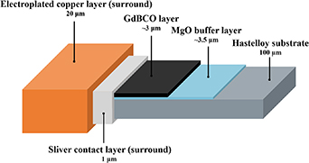
Figure 1. Sectional structure of the HTS tapes.
Download figure:
Standard image High-resolution imageTable 1. Specifications of the tape.
| Specifications | Values |
|---|---|
| Width | 6 mm |
| Thickness | ∼170 μm |
| Critical current (77 K, self-field) | 290 A |
| n-value | >25 |
2.2. Fabrication process for the tape in semi-PCS
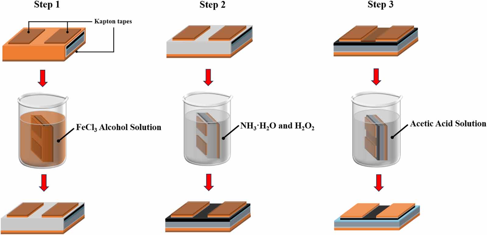
The processing steps of the HTS tape are shown in figure 2 and can be divided into three steps. In the first step, Kapton tapes are used to cover the copper layers that need to be retained, leaving the rest of the copper layers uncovered. As shown in figure 2, the superconducting side of the HTS tape is covered with two segments of Kapton tapes, exposing the center and periphery, and the non-superconducting side is covered entirely with a Kapton tape. In addition, the width of the Kapton tapes needs to be slightly narrower than the width of the HTS tapes to expose the copper layer at the edges. In this study, 5 mm wide Kapton tapes were used for the 6 mm wide HTS tape. Then, a FeCl3 alcohol solution is used to remove the uncovered Cu layer on the tape surface and edges. In the second step, a mixture of NH3·H2O and H2O2 is used to remove the uncovered silver stabilizing layer of the tape. The critical current of HTS tape subjected to chemical etching can remain unchanged [15]. The FeCl3 alcohol solution is prepared by mixing and dissolving FeCl3 powder with a mass fraction of 98% and alcohol solution with a mass fraction of 99.7% at a ratio of 1 g:20 ml. The NH3·H2O and H2O2 mixed solution is prepared by mixing NH3·H2O with a mass fraction of 28% and H2O2 with a mass fraction of 30% [16]. The two steps are both cost-effective and highly efficient for removing Cu and Ag materials that maintain electrical connections between superconducting and non-superconducting surfaces.

Figure 2. Procedure used to remove part of Cu stabilizer, Ag protective and superconducting layers in the HTS tape.
Download figure:
Standard image High-resolution imageThe buffer layer of the HTS tape may be wrapped with the superconducting layer on the edges during mass production. In order to prevent current conduction on superconducting and non-superconducting sides at temperatures below the superconducting critical temperature through the superconducting layer wrapped on the edges, it is necessary to remove the superconducting layer that may be covered on the edges of the HTS tape. It is achieved in the third step by reacting them with an acetic acid solution. In this step, it is necessary to cover the GdBCO layer that has been exposed in the middle section of the tape with a Kapton tape to prevent this section from being corroded by acetic acid, and then the tape is put into the acetic acid solution to react. The reaction removes the GdBCO that may be wrapped around the buffer layer edges of the HTS tape. As a result, the electrical connection between the two surfaces of the tape is cut off, ensuring that almost all of the current flows on the GdBCO layer. Due to the buffer layer beneath the GdBCO layer being essentially insulating and the relatively high resistance of the GdBCO layer when not in the superconducting state, the entire semi-PCS shows a high switching-off resistance.
2.3. Semi-PCS configurations
Figure 3 shows the semi-PCS configurations for this study. The dark part in the middle of the tape is the GdBCO layer, where Cu and Ag layers have been removed. The shadow part around the tape is the buffer layer, where Cu, Ag and GdBCO layers have been removed. The critical temperature of the HTS tape is approximately 93 K. We defined that semi-PCS 'off' when it is at 110 K. A type E thermocouple in the center of the semi-PCS is used to collect temperature data, which is connected to the temperature controller to determine whether it is 'on' or 'off.' A nickel–chromium wire (Ni80Cr20) is used as the heating source and is connected to a DC power supply. The nickel–chromium wire transfers the heat generated to the HTS tape by conductive heat transfer. Voltage taps were installed near the ends of the foam to monitor the semi-PCS resistance during the heating experiments. To improve the heat transfer efficiency, the HTS tape and the nickel–chromium wire were uniformly coated with cryogenic thermally conductive grease (i.e. Apiezon N grease). The HTS tape and the nickel–chromium heater were closed by two extruded polystyrene (XPS) foams with poor thermal conductivity to create a 'heat trap' to store the heat. The XPS foams were sealed by low-temperature adhesive. We placed the semi-PCS unit in a large foam container for 77 K operation in liquid nitrogen (LN2).
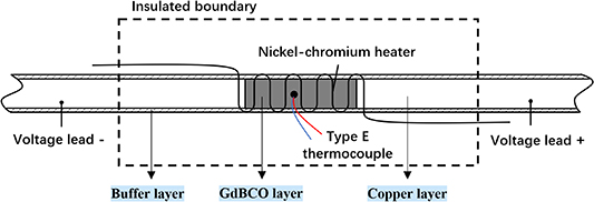
Figure 3. Semi-PCS configurations.
Download figure:
Standard image High-resolution image2.4. Coil with high switching-off resistance semi-PCS configurations
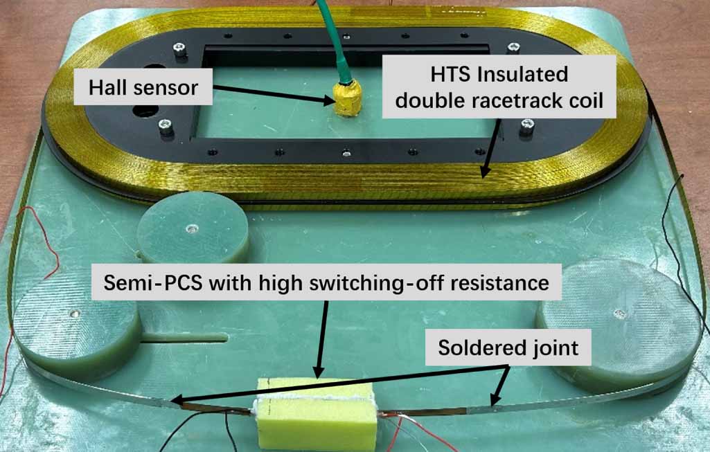
Figure 4 shows the general arrangement of our insulated coil with designed high switching-off resistance semi-PCS, which was used for the excitation experiments to verify the effectiveness of the semi-PCS. The HTS coils were wound using HTS tapes with an average critical current of 198 A. The HTS tape is 6 mm in width, 180 μm in thickness, and the total length of the coil is 128 m. In this study, Kapton tapes with a width of 6 mm and a thickness of 50 μm were used for insulation. After the HTS coil was wound, its inductance was measured to be 5.6 mH using a TH2811D LCR Meter. Note that the HTS coil and semi-PCS are connected via two soldered joints. The superconducting side of the semi-PCS tape and the superconducting side of the coil tape are soldered by a thin layer of low-temperature soldering tin between them to form a joint with a resistance of about 10 nΩ. Since superconducting joint technology was not adopted in making this HTS coil, the coil operates in a semi-persistent mode. To ensure no accidental burning of the semi-PCS during switching, we chose a liquid nitrogen bath (LN2, 77 K) as the experimental environment. An Agilent 34 420 A digital nano voltmeter was connected to both ends of the coil to measure the voltage, including the voltage generated by the semi-PCS and the joints. The source current, controlled by a LabVIEW program, was generated by an Agilent 6680 A power supply. The magnetic field was monitored using a Gaussmeter (Lake Shore Model 425 with a resolution of 0.01 mT) with a Hall sensor (Lake Shore HGCA-3020) inserted in the center of the coil.
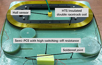
Figure 4. Coil with designed high switching-off resistance semi-PCS configurations.
Download figure:
Standard image High-resolution image3. Results and discussions
3.1. Microstructure of the tape of the high switching-off resistance semi-PCS
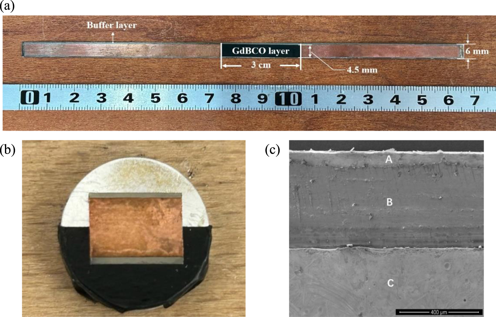
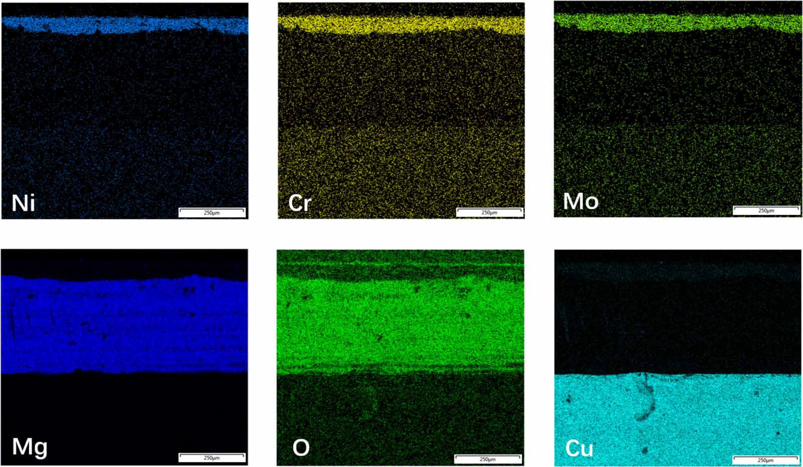
The HTS tape specimen subjected to a three-step treatment described in section 2.2 is shown in figure 5(a). The length of the specimen is approximately 17 cm, with an exposed GdBCO layer measuring around 3 cm in length and 4.5 mm in width. In order to examine the microstructures of the treated tape, a section was taken out from it, shown in figure 5(b), and observed under scanning electron microscopy (SEM, NOVA NanoSEM 230). Figure 5(c) illustrates the three areas (A, B, and C) at the tape's edge. To further verify the elemental composition of each area, energy dispersive spectroscopy (EDS) was used to analyze the elemental compositions. As shown in figure 6, the tape's edge layer area A has the main composition of Ni, Cr, and Mo, so it is the Hastelloy substrate layer. Area B is the main composition of Mg and O, so it is the buffer layer, and area C is the copper layer. The results show that the copper, silver and superconducting layers have been clearly removed, which can prevent current flow between the superconducting and non-superconducting sides of the tape. This guarantees that the semi-PCS has high resistance in off-state.

Figure 5. (a) The top view and length of the treated tape. (b) A section of the treated tape. (c) SEM view of the treated tape.
Download figure:
Standard image High-resolution image
Figure 6. EDS images of the treated tape.
Download figure:
Standard image High-resolution image3.2. Critical current test and switching-off resistance measurement of the semi-PCS
In order to determine the electrical characteristics of the HTS tapes treated in the three steps mentioned in section 2.2 and assess the reliability of the production process, we fabricated a semi-PCS sample. It was then subjected to three cycles of heating up to 110 K and cooling down to 77 K. The critical current of the semi-PCS was measured using the four-probe method. Figure 7 shows representative I–V curves for the semi-PCS and the original tape used as a reference. The n-value of the treated tape did not change compared to the original tape, but the critical current reduced by approximately 26%. This reduction can be attributed to the shorten in the width of the superconducting layer after etching with acetic acid, from 6 mm to around 4.5 mm. So, the reduction of the critical current can be considered reasonable, indicating that the chemical etching in steps 1, 2 and 3 did not cause damage to the GdBCO layer of the HTS tape. It is necessary to point out that even though the critical current of the tape decreases, the semi-PCS is typically located far from the center of coils and experiences a relatively weak magnetic field, so the critical current of the tape for making semi-PCS would be much larger than the critical current of the HTS coil. Furthermore, the semi-PCS exhibited no critical current decay across multiple warming and cooling thermal cycles, suggesting it suitability and reliability for applications in the HTS magnets.
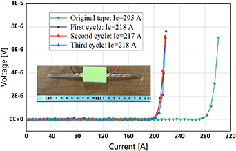
Figure 7. I–V curves of the treated HTS tape. The I–V curve of the original HTS tape is also plotted as reference. The inset is the semi-PCS used for the measurements.
Download figure:
Standard image High-resolution imageThe resistance of the semi-PCS in the off-state was tested subsequently. Figure 8(a) shows the transient response of the prototype semi-PCS with the heater submerged in the LN2 bath. Applying 1.67 W of power to nickel–chromium wire in the semi-PCS required a hold time of about 2 min to open it. The temperature measured by thermocouples during the test was about 111 K. By soldering two voltage leads, the resistance of the semi-PCS at 111 K can be measured to be 1.18 Ω, which is much larger than the resistance in the common heater-triggered semi-PCS [8, 13, 17], which are normally in the mΩ level. The change of resistance exhibits a delay during both the warming-up and cooling-down stages. Specifically, the resistance begins to change when the temperature reaches around 100 K during warming up, while it rapidly returns to zero resistance during cooling down. The delay is caused by the thermocouple being in contact with the nickel–chromium heater (i.e. the thermocouple does not contact to the HTS tape directly). This contact may lead to a higher measured temperature than the actual temperature of the HTS tape during the warming-up stage.
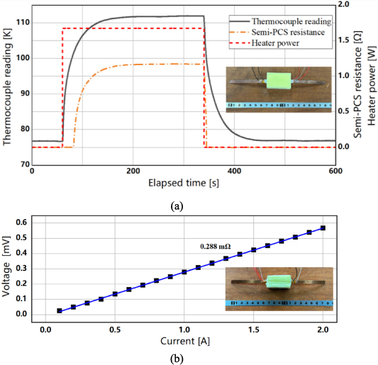
Figure 8. (a)The transient response of the semi-PCS during operation, showing the temperature rise measured by the thermocouple vs elapsed time, along with HTS tape resistance and heating power. (b) I–V curve of semi-PCS made of the unetched tapes at 111 K.
Download figure:
Standard image High-resolution imageFurthermore, a semi-PCS of the same size as the previous one using the same THEVA tape without etching was also made, and the voltage taps and heater arrangements were the same. Figure 8(b) shows the I–V curve of this semi-PCS at 111 K. The voltage is linearly proportional to the current, indicating that the semi-PCS is resistive. By determining the slope of the line, we can calculate the resistance of the semi-PCS made of the unetched THEVA tapes at 111 K as 0.28 mΩ. So, the switching-off resistance of the semi-PCS made of etched tapes in the off-state is improved by over 4000 times compared to that of unetched tapes.
3.3. Coil energization
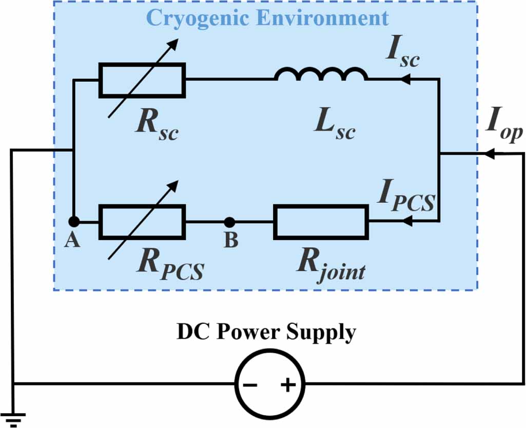
Figure 9 shows the equivalent circuit model corresponding to this experiment. Iop is the source current supplied by the DC power supply; Rsc and RPCS denote the coil resistance and the semi-PCS resistance, respectively; the voltages generated by Rsc and Rpcs are described by the E-J power law equation; IPCS , Isc , Lsc, and Rjoint are the currents in the semi-PCS, the currents charging the coils, the coil inductance, and the joint resistance, respectively. The voltage between points A and B is defined as UPCS.
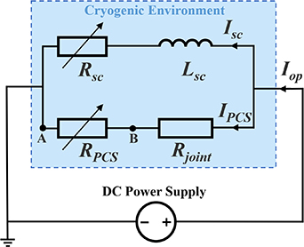
Figure 9. Equivalent circuit of the closed-loop HTS coli with a PCS.
Download figure:
Standard image High-resolution imageFigure 10 shows the experimental and simulation results of insulated coil excitation. The excitation rate is set to 1 A s−1, and the excitation target current is 20 A for test. At the beginning of the charging process, since the impedance of the semi-PCS is much larger than that of the coil, only a minimal amount of Iop flows through the semi-PCS, and most of the Iop flows into the coil. The distribution of the currents in the semi-PCS and the coil is inversely proportional to the ratio of their impedances. After about 20 s, the IPCS and Isc stabilize. The observed voltage across the coil of 5.7 mV during charging corresponds to the calculated coil inductance multiplied by the current ramp rate, and the measured magnetic induction of 14.5 mT at a current of 20 A is within 1% different from the expected value. The difference between the experimental and simulation results may be due to measurement errors because IPCS is calculated from UPCS, and Isc is calculated by subtracting IPCS from Iop. The experiment is used to verify the validity of the high switching-off resistance semi-PCS proposed in this paper and the correctness of the simulation model.

Figure 10. Experimental and simulation results of the insulated coil excitation.
Download figure:
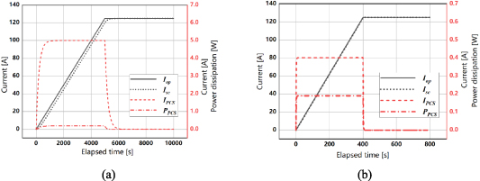
Standard image High-resolution imageIn order to further describe the advantages of the semi-PCS proposed in this paper, the simulation model mentioned above is utilized on a large insulated coil. The data used in this study is obtained from [18], where the HTS insulated coil was constructed by connecting six single pancake coils in series. Each coil consists of 335 turns, resulting in a total of 2010 turns and an inductance of 1.52 H. The excitation target is set to 125 A for safety. Figure 11 shows the excitation results of the proposed semi-PCS and the conventional PCS for generating the same power dissipation. The results show that when both the PCSs generate 0.19 W power dissipation, the semi-PCS proposed in this paper takes only 400 s to complete the excitation, and the excitation speed reaches 0.31 A s−1, while the conventional PCS takes 5000 s, and the excitation speed can only reach 0.025 A s−1. Notably, the heater-triggered PCS requires continuous heating to sustain its off-state. Therefore, increasing the speed of excitation can minimize heat input, effectively reducing the thermal load of the magnet system.
Figure 11. Excitation results (a) the proposed semi-PCS (b) the conventional PCS.
Download figure:
Standard image High-resolution image
In addition, the size of the semi-PCS in this paper is also much smaller than the PCS in [18], which uses a 1300 mm HTS tape, while only a 170 mm HTS tape is used in this paper, and the tape encapsulated in the adiabatic foam is only 50 mm. The smaller PCS implies a minor enthalpy change from 'on' to 'off,' which can shorten the switching time, which is also crucial for the efficiency of operations of the HTS magnets.
Advantages of this proposed semi-PCS include (1) a simple fabrication process, (2) very high resistance in the off-state (i.e. ohmic level), and (3) minimizing the heat burden while charging the coil. Nevertheless, the semi-PCS proposed in this paper has its limitations. It requires a high level of tape manufacturing process. Some tapes have defects in the buffer layer [19], which can lead to current flow from the superconducting side to the non-superconducting side through buffer layer and cause the switching-off resistance of the semi-PCS to be dominated by the resistance of the Hastelloy layer. In addition, a parallel protection resistor alongside the semi-PCS is still necessary in practical applications, which helps to release the energy in the magnet coils in case of an unexpected quench in the semi-PCS, enhancing the safety of the magnet's closed-loop operation [20].
4. Conclusion
We successfully fabricated an HTS semi-PCS with high switching-off resistance by removing part of the conductive and superconducting layers on the HTS tape surface and edges. The resistance of the proposed semi-PCS in the off-state is improved by over 4000 times compared to the conventional heater-triggered semi-PCS using the same length and width of the original Cu-stabilized tape. This improvement in switching-off resistance makes the proposed semi-PCS highly efficient for large closed-loop HTS magnets' charging since it significantly increases the excitation speed with low power dissipation. Therefore, the proposed semi-PCS shows a great potential for the large inductance magnets applications.
Acknowledgments
This work was funded by the National Natural Science Foundation of China (Project No. 52037008), the National Natural Science Foundation of Shanghai (Project No. 20ZR1425800), and the Shanghai Rising-Star Program (Project No. 20QC1401400).
Data availability statement
All data that support the findings of this study are included within the article (and any supplementary files).