
Abstract
Understanding the magnetic field sensitivity of transition edge sensors (TESs) is vital in optimising the configuration of any magnetic shielding as well as the design of the TESs themselves. An experimental system has been developed to enable the investigation of the applied magnetic field direction on TES behaviour, and the first results from this system are presented. In addition, measurements of the effect of applied magnetic field magnitude on both supercurrent and bias current are presented. The extent to which the current theoretical framework can explain the results is assessed and finally, the impact of this work on the design of TESs and the design of magnetic shielding is discussed.
Export citation and abstract BibTeX RIS

Original content from this work may be used under the terms of the Creative Commons Attribution 4.0 license. Any further distribution of this work must maintain attribution to the author(s) and the title of the work, journal citation and DOI.
1. Introduction
Transition edge sensors (TESs) have become a crucial technology in a number of fields of research. TESs are used as high-resolution energy-resolving detectors for x-rays [1, 2], optical photons [3], electrons [4], neutrinos [5] and dark matter candidates [6] in areas such as particle physics, astronomy and quantum cryptography. They are also used as highly sensitive power detectors for photon fluxes in mm, sub-mm and far-infrared astronomy [7, 8]. As a result, there is significant interest in understanding factors that can affect and degrade TES operation.
One such factor is magnetic field sensitivity. Magnetic field sensitivity means TESs must be shielded from stray and/or time-varying fields that might arise in operation. Sources include electric currents, both in the surrounding wiring and in the TESs themselves [9], components of the cooling system such as cryo-compressors [10] or adiabatic demagnetisation refrigerators (ADRs) [11], or other parts of the instrument for example the beam deflectors in a telescope or motors driving rotating polarizing plates.
Trade-offs are involved in the design of the shielding. For example, to couple the TES detector to the desired signal (photons, x-rays etc), to allow electrical connection to the external warmer electronics, or to allow thermal connection to the cooling platform, the magnetic shielding must be engineered to include apertures, through which static and low frequency magnetic fields may penetrate [12]. In space-missions the level of shielding may have to be traded-off against weight. In these situations, it is critical to understand the magnetic field sensitivity of TESs in detail, so that performance of the design can be assessed and optimized [13]. The scale of the field sensitivity is obviously critical to determine minimum shielding levels. Directionality of the sensitivity is also important, e.g. in constraining the orientation of apertures for apertures for optical access or wiring or the routing of harnesses harnesses with respect to the TES. In other circumstances it may be desirable to operate TESs in a magnetic field when an understanding of the likely effect of the magnitude and orientation of the field is also crucial. By contrast, recent measurements show that TESs are insensitive to applied electric fields [14]. Here we report a systematic experimental study of the effect of applied magnetic field and its orientation on a range on TES operating parameters and derived characteristics (critical current, bias current, transition temperature, power-to-current responsivity) as a function of TES lateral dimensions and geometry.
A TES is sensitive to magnetic field by virtue of its geometry. At a fundamental level, a TES comprises a superconductor  , often chosen to have with a superconducting critical temperature
 1 K, connected to readout electronics by thin film wiring made from a superconductor
  having a higher Tc. The TES operates within the superconducting-normal resistive transition of
  .
.  is typically a superconducting thin-film or superconductor-normal metal (S/N) bilayer with thickness ∼100 nm, and lateral dimensions ∼10 µm. Wiring layer
  is a higher Tc superconductor typically Nb such that
  ∼8 K. The combination
  forms a superconducting weak-link due to the superconducting proximity effect [15]. In many practical TES designs additional normal metal structures are added on top of
  in order to improve other aspects of behaviour such as structures along the longitudinal edges ('banks') to address possible imperfections or lateral 'bars' added across the direction of current flow. Previous work has shown that adding banks can reduce B-field sensitivity [16], as does reducing the spacing of any bars [17].
Observation of the Josephson effect above the intrinsic transition temperature of  in TESs is now well-established experimentally [16, 18]. It is also well-established that both the effective Tc and superconducting critical current
  in weak links are sensitive to the magnitude of a magnetic field (B) applied in the direction normal to the plane of the TES. Measurements of
  with B perpendicular to the TES exhibit an oscillatory, Fraunhofer-like dependence. Broadly similar oscillations have been observed in the bias current of the TES Ib
under voltage-bias [19–22]. The small-signal electrothermal parameters that characterise the change in TES resistance (R) with temperature (T) and current (I),
with B perpendicular to the TES exhibit an oscillatory, Fraunhofer-like dependence. Broadly similar oscillations have been observed in the bias current of the TES Ib
under voltage-bias [19–22]. The small-signal electrothermal parameters that characterise the change in TES resistance (R) with temperature (T) and current (I),  and
and  [23] also exhibit oscillatory behaviour with magnetic field [24]. Changes in α and β are expected to change the small-signal power-to-current responsivity, and therefore the noise equivalent power for bolometric applications and the achievable energy resolution for calorimetric applications [19]. A review of the current understanding of TES physics is given by Gottardi and Nagayashi [25].
This paper presents an experimental study of the effect of magnetic field magnitude and orientation on a set of MoAu TESs as a function of TES lateral dimensions. Although we would expect some dependence of these effects on TES materials for other lead/bilayer combinations and operating temperatures, the physical origin of the magnetic field sensitivity discussed above must make our observations generic. Section 2 describes the experimental method, including a description of the TES geometry, the three-axis magnetic field system, device materials and fabrication processes. Section 3 gives details of the measurements. For convenience, these are categorised by the type of measurement carried out. Section 3.1 shows the effect on supercurrent of a magnetic field applied perpendicular to the plane of the TES. Section 3.2 then presents the temperature dependence of the supercurrent for a subset of the TESs studied here, showing the effects of device size. Section 3.3 describes measurements of the effect of applied field on the current in the TESs studied here under voltage bias, including a first-order estimate of the effect on TES responsivity. Section 3.3.3 gives details of measurements of the dependence of the bias current of voltage-biased TESs as a function of the orientation of an applied magnetic field. Section 4 discusses the measurements and concludes with recommendations for the use of TESs in a magnetic field.
2. Experimental method
The measurements were made on a set of Mo/Au bilayer TESs with Nb wiring that were specifically fabricated to explore a range of device geometries with TES areas varying from 5 µm × 5 µm to 70 µm × 70 µm. Unless otherwise noted, in all devices tested the bilayer was thermally isolated from the substrate by suspending it on a 200 nm thick SiN island in a well on four 1.4 µm wide and 50 µm long beams (or 'legs'). The thermal conductance between the TES and the substrate was designed to be  2 pWK−1. Optical micrographs of representative devices are shown in figure 1.
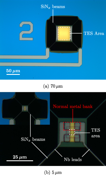
Figure 1. Photos of the (a) largest and (b) smallest device tested here. The TES area, the region used to define the bilayer side length, is indicated by the dashed white square in both photos. The SiN beams supporting the membrane are also labelled. Normal metal banks and superconducting contacts are indicated in the close-up photo of (b).
Download figure:
Standard image High-resolution imageThe TESs were processed on Si wafers coated with a membrane layer comprising 200 nm thick LPCVD SiN grown on top of a 50 nm thermal thick SiO2 etch-stop layer. Reactive-ion etching was first used to define the device wells, islands and support beams in the front- and backside membrane layers. This was followed by deposition of the metal layers, in each case by DC magnetron sputtering. The Mo/Au bilayers were deposited first and patterned using a two-stage wet etch process. 120 nm of Au was deposited on top of 40 nm of Mo, targeting  ∼ 180–200 mK. Next a lift-off process was used to pattern additional 200 nm thick Au normal metal features, such as banks and bars, on top of the bilayers. A lift-off process was then used to pattern a 200 nm thick Nb wiring layer. Finally, the device membranes were released from the substrate by using deep reactive ion etching (DRIE) to remove the underlying Si. This etch was carried out from the back-side of the wafer and terminated on the SiO2 etch stop layer [26].
Images of the largest and smallest TES tested are shown in figure 1. The white dotted lines in both images indicate the nominal TES dimension and we identify the TESs in terms of the length of this region L. Figure 1(a) highlights the key features of a 5 µm TES. The red dotted lines show the outline of one of the longitudinal metal banks. Nb leads and two of the  beams are also indicated.
Figure 2 shows the general geometry and notation used to describe the components of the TESs. We assume that current flows in the longitudinal (x) direction between the two superconducting electrodes,  (shown in red). The (blue) structures labelled
  are the 200 nm normal metal banks deposited across the longitudinal edge of the bilayers. These strongly suppress the superconductivity of the underlying bilayer, giving a clean boundary between normal and superconducting regions at the bank edge; in this way irregularities associated with the edge of the bilayer are avoided. The bilayer area
  (shown in yellow) left uncovered by banks and wiring was square in all cases and its side-length L is used to here define the size of the TES. In addition, for some TESs partial lateral normal-metal bars (the paler blue features) were added in the same deposition step as the longitudinal banks. Two such bars are indicated by the dotted lines in the diagram in figure 2. The addition of the normal metal features on the longitudinal edges also creates a lateral proximity effect. The lower plots sketch typical representative spatial variations of the superconducting order parameter in all three dimensions [15].

Figure 2. Schematic of the TES structure with leads and banks illustrating the proximity effects involved. The superconducting leads (red) are labelled  , the thin film TES bilayer (yellow) is
  and the side banks (blue) are
  . The dashed (blue) lines and shading indicate normal metal bars, included on some of the devices. These were the same thickness as the side banks. The regions
  and
and  were composed of a superconductor
  of uniform thickness and a normal metal
  , whose thickness differed between
  and
and  . Representative variations of the order parameter, a measure of the superconductivity, are indicated beneath the schematic as a function of position in the x, y and z directions.
Download figure:
Standard image High-resolution imageThe TESs were mounted in the box shown in figure 3 for testing. This incorporated a three-axis Helmholtz arrangement, with three pairs of current-carrying coils mounted on the sides of a cube. The mechanical design of the assembly ensured that the TESs were located at the centre of the coils, with the plane of the TESs normal to Bz and the longitudinal axis parallel to Bx . This magnetic coil arrangement is not a true Helmholtz 3-axis arrangement, since each pair of coils is separated by a distance equal to their diameter instead of their radius. However, the expected field in the 5 mm by 5 mm region in the centre of the cube occupied by the devices was simulated and shown to be uniform to within 2%–3%. The magnitude of the applied field in each direction was calibrated using a Lakeshore cryogenic Hall probe [27].
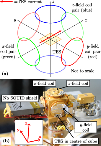
Figure 3. (a) Schematic showing the Helmholtz coils and TES orientation. The TESs were mounted with the plane of the TES perpendicular to the z axis and the direction of current flow parallel to the x axis. (b) Completed test unit mounted on an ADR. The SQUIDs are mounted in the niobium magetic shield indicated on the left of the figure. The field coils are indicated. The coordinate axes, here depicted in red, are used to describe the direction of the applied magnetic field.
Download figure:
Standard image High-resolution imageThe TESs were read-out using two-stage superconducting quantum interference devices (SQUIDs) supplied by Magnicon [28]. The SQUIDs were mounted parallel to the x − y plane as indicated in figure 3 close to the TESs, but surrounded by a machined Nb shield to ensure that their operation was not affected by the operation of the magnetic field system. At the maximum magnetic field used, the change in the measured SQUID current corresponded to a variation in TES current of 30 nA. With TES bias currents of the order of µA, this effect was not significant.
The TESs and SQUID electronics were cooled to operating temperature using a two-stage ADR launched from a pulse-tube cooled 4 K stage. The base temperature of the system was ∼65 mK.
3. Results
3.1. The effect of magnetic field on critical current
Here we describe measurements of the TES critical current  with magnetic field Bz
normal to the plane of the TESs. For these measurements the bath temperature was regulated at a temperature close to
with magnetic field Bz
normal to the plane of the TESs. For these measurements the bath temperature was regulated at a temperature close to  to better than ± 0.1 mK. For clarity here and in what follows, we identify individual TES characteristics particularly
  with an additional subscript e.g.
  to indicate that measurements apply to a specific device. Our measured
  varied with TES size. For each applied field, and each TES the bias voltage Vb
was swept symmetrically about Vb
= 0 V and
varied with TES size. For each applied field, and each TES the bias voltage Vb
was swept symmetrically about Vb
= 0 V and  determined from the device current at the first onset of resistance for both positive and negative bias directions. The voltage sweep was carried out at a sufficiently low rate of 0.3 Hz to avoid thermal hysteresis, similar to Smith et al [19].
Assuming that the supercurrent density is uniform, a magnetic field Bz is expected to modulate the TES critical current such that [19]

Here  is the critical current at zero field,
  is the magnetic flux through the plane of the TES and Φ0 is the magnetic flux quantum.
  is an effective TES area defined further below. The variation of
  is then the same as the Fraunhofer diffraction pattern. Equation (1) suggests that a smaller TES is less sensitive to a normal magnetic field Bz
.
is then the same as the Fraunhofer diffraction pattern. Equation (1) suggests that a smaller TES is less sensitive to a normal magnetic field Bz
.
It is necessary to assume a value of Aeff to convert the known applied field to the flux  . For a TES with order parameter modified by the proximity effect as shown in figure 2, it is not obvious that the effective area
  for the flux calculation is the same as the geometric bilayer area A, as indicated in figure 1(b). In particular, it might be expected that the contribution to Aeff from a particular area element will scale with the value of the superconducting order parameter at that point. The approach we take here is to instead determine Aeff for a given device as the area giving the best account of the central peak of the measured supercurrent oscillations. From the effective area we can define an effective side length
  .
.
Figure 4 shows the effective length calculated in this manner plotted as a function of true length for all of the devices tested in this study. For unpatterned devices with no bars the effective length is always smaller than, but comparable with, the actual length, with greater deviation seen for larger devices. The behaviour for devices with bars is more complicated and will be discussed in subsequent sections.

Figure 4. Effective length, corresponding to the effective area determining by fitting (1) to the Ic vs B data, as a function of true length. Black asterisks show data for unpatterned devices, red crosses show devices with a single partial bar, blue diamonds show devices with two partial bars and green circles show devices with three partial bars.
Download figure:
Standard image High-resolution image3.1.1.
 for unpatterned devices.

Figure 5 shows the measured normalized critical currents  as a function of magnetic flux for a series of unpatterned TESs with different bilayer side lengths in the range 5–70 µm. The solid lines show the fitted dependence of
  as given by equation (1). Measurements for each TES are plotted with a vertical offset of 0.5 between datasets where the coloured-matched dashed lines indicate the y-axis zero in each case. For the smaller devices, 20 µm side length and below, very good agreement is shown with the prediction, whilst the larger devices are less well described. In particular, the larger devices do not show well-defined minima in
  when the flux is an integer of flux quanta.
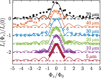
Figure 5. Critical current as a function of magnetic flux, calculated using the effective area that gives the best fit to the oscillations in  , for a series of unpatterned TESs with different bilayer side lengths. Measurements for each TES are plotted with a vertical offset of 0.5 between datasets where the colour-matched dashed lines indicate the y-axis zero in each case. Each set of measurements was taken just below the transition temperature of the TES under test. All data sets have been normalised to
  at zero flux. The solid lines show the prediction of equation (1).
Download figure:
Standard image High-resolution image3.1.2. Effect of partial lateral bars on .

Figure 6 shows the measured the critical current as a function of magnetic flux for a series of TESs with 10 µm bilayers and increasing numbers of bars. Again the colour-matched horizontal dashed lines indicate the y-axis for the offset data sets. The currents have been normalised to  at zero flux and the magnetic flux has been calculated using the effective area that gave the best fit to the periodic structure in critical current. At first sight, figure 6 shows the expected Fraunhofer-like dependence of
  with Φ for all of these 10 µm TESs. However, we find a clear difference between behaviour of
  for between even and odd numbers of bars. For even numbers of bars
  for integer m, as expected from equation (1). For odd numbers of bars we instead find
  for integer m, i.e. although they are local minima in the critical current, the points
  for integer m are not the expected nulls.
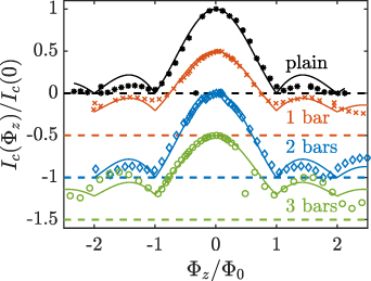
Figure 6. Critical current as a function of magnetic flux through the bilayer for a series of 10 µm devices patterned with different numbers of normal metal bars. All data sets have been normalised to  at zero flux, and each set of measurements was taken just below the transition temperature of the TES under test. The data are plotted with a vertical offset of 0.5 between datasets. The solid lines for the unpatterned TES and the TES with two bars show the prediction of equation (1) whilst the solid lines for TESs with one and three bars have been fitted using equation (2). Again the colour-matched horizontal dashed lines indicate the y-axis for the offset data sets.
Download figure:
Standard image High-resolution imageEmpirically we found that the behaviour of the critical current for odd numbers of bars could be well described by modifying equation (1) with the addition of a quadratic term:
where  and aj
are parameters of the model. The solid lines shown in figure 6(a) for 1 and 3 bars use a1 = 0.7 and a2 = 0.005. Despite the evidently different behaviour of
and aj
are parameters of the model. The solid lines shown in figure 6(a) for 1 and 3 bars use a1 = 0.7 and a2 = 0.005. Despite the evidently different behaviour of  with bar number, all four TESs have similar effective lengths, as seen in figure 4.
The dependence of  on number of bars may arise from the geometry of the supercurrent flow in the different cases. Measurements on identical TESs with lateral bars that completely crossed the
  region have been carried out by Harwin et al [29]. These showed that the bar/bilayer structure itself remained in the normal state to temperatures at least to 80 mK, i.e. well below the temperatures of interest here, and with zero measurable supercurrent, despite the proximity of the bilayer. This implies negligible supercurrent current flow across the bars themselves, so partial bars should result in a meandering supercurrent pattern.
The self-magnetic field generated in the TES by a meandering current can be understood using a simplified Biot-Savart law calculation. Figure 7 shows Bz produced by a current of 5 µA following the path shown in red. Figure 7(a) shows the case with two normal metal bars and figure 7(b) the case with three normal metal bars. Critically, it can be seen that sign of the self-field alternates between adjacent current loops.
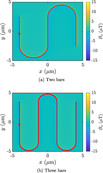
Figure 7. Calculated magnitude of the component of magnetic field perpendicular to the TES thin film, over the surface of the film, produced by a current of 5 µA following the path shown in red. (a) and (b) illustrate the effects of differing numbers of normal metal bars, as the normal metal bars determine the pattern of current flow.
Download figure:
Standard image High-resolution imageThe self-flux is the sum of the flux in each of these loops and adds to the applied flux, modifying the behaviour of Ic. With an even number of bars and therefore loops, we expect the sums of fluxes in adjacent pairs of loops to cancel; hence the self-field correction will be negligible. For an odd number of bars there is one unmatched loop, leading to a finite self-flux correction. Further, the scale of the correction should decrease as the applied B-field is increased and the self-field becomes less significant. This behaviour is consistent with the data.
Figure 8 shows the measured effect of adding three partial normal metal bars to a larger TES with a side length of 40 µm. The Fraunhofer pattern in  is evident for the device without bars, although the expected minima with Φ are not well defined. In the device with three bars the Fraunhofer pattern is absent and Ic
is almost independent of
is evident for the device without bars, although the expected minima with Φ are not well defined. In the device with three bars the Fraunhofer pattern is absent and Ic
is almost independent of  up to
up to  . We explore this effect further in section 3.3.2.

Figure 8. Critical current as a function of magnetic flux through the bilayer for two devices with 40 µm side-length bilayers, one unpatterned and one with three partial normal metal bars. Both data sets have been normalised to  at zero flux, and each set of measurements was taken just below the transition temperature of the TES under test. The data are plotted with a vertical offset between datasets of 1.5. The solid lines show the prediction of equation (1).
Download figure:
Standard image High-resolution image3.2. Temperature dependence of in zero field

Figure 9(a) shows the critical currents of three of the smallest unpatterned TESs in zero field as a function of Tb
. Figure 9(b) shows the same data and fits but expands the region around  . The black lines show the expected temperature dependence of the current in a SS'S weak-link for
  given by both Golubov [30] and Sadleir [18]
with  . For the three TES lengths, we find a value ξi
= 450 ± 20 nm and
. For the three TES lengths, we find a value ξi
= 450 ± 20 nm and  = 197 ± 3 mK. This gives an excellent account of the measured supercurrents in this regime. Below
  , Ic
is well accounted for by the expected Ginzburg–Landau dependence
, Ic
is well accounted for by the expected Ginzburg–Landau dependence  . This dependence is shown by the dashed black line in figure 9(b) for the 20 µm TES. Using a free electron model with Fermi velocity
  = 1.39 × 10⁶ ms−1, and the measured resistivity for our 120 nm thick Au films ρ = 1.33 × 10⁻⁸ Ωm, we calculate a normal-state electronic diffusion coefficient D = 2.80 × 10⁻² m2s−1. Using
  , we calculate ξn
= 450 nm, in good agreement with the measurement. These observations are consistent with [18] and we identify
, we calculate ξn
= 450 nm, in good agreement with the measurement. These observations are consistent with [18] and we identify  .
.
Figure 9.
 for three TESs of different bilayer side lengths. All measurements were taken with zero applied field. (a) Shows all data and fits, (b) provides more detail of the region near
  . The solid lines show the expected current for a SS'S weak-link for
  for all three data sets, whilst the dashed black line for the 20 µm data show the expected Ginzburg–Landau dependence below
  for the 20 µm TES, the dashed vertical line in the lower plot.
Download figure:
Standard image High-resolution image3.3. Effect of field on voltage-biased TESs
Sadleir et al [16, 18] investigated the variation of measured  with geometry and field for TESs at temperatures
  where
where  is the temperature corresponding to the mid-point of the resistive transition,
  . Those measurements were performed on unreleased TESs, for which the thermal conductance to the heat bath is high and TES Joule power heating with current bias
  is relatively unimportant for low bias currents Ib
. Here we report
is relatively unimportant for low bias currents Ib
. Here we report  for TESs with thermal isolation from the substrate under voltage bias using the measured bias power at
  as a function of applied field in order to determine
  . This approach explicitly explores the operating regime of a TES under voltage bias.
Figure 10 shows measurements of the TES Joule power determined at  for an unpatterned TES with 70 µm side length. These
  curves were parametrized using
  , assuming that parameters K and n, that describe the heat flow to the heat bath [23] at temperature Tb
, do not change with field for a particular TES. This procedure was used to determine
, assuming that parameters K and n, that describe the heat flow to the heat bath [23] at temperature Tb
, do not change with field for a particular TES. This procedure was used to determine  for a range of TES lengths. The inset of figure 10 shows example
  curves at three different applied magnetic fields for this TES, all measured at fixed Tb
= 75 mK. The
curves at three different applied magnetic fields for this TES, all measured at fixed Tb
= 75 mK. The  plot at the maximum field shown here, B = 50 µT, would correspond to
  , well-beyond the range of data shown in figure 5.
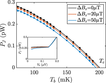
Figure 10.
 curves for different applied fields, measured for an unpatterned TES with 70 µm side length.
  was determined at
  . The inset shows sample
  curves at the same applied magnetic fields, all measured at Tb
= 75 mK.
curves at the same applied magnetic fields, all measured at Tb
= 75 mK.
Download figure:
Standard image High-resolution imageInterestingly, although the field-dependent maxima of the supercurrents shown in figure 5 closely-follow the expected Fraunhofer-like dependence, the Joule power for the voltage-biased TES is changed only modestly (∼5%) with B. Additionally there is evidence of change in the overall  with B that would be consistent with reduced α with increasing field.
Figure 11 shows how  changes with applied field Bz
. Figure 11(a) shows
changes with applied field Bz
. Figure 11(a) shows  for three unpatterned TESs with geometric length
  20 µm.
  is reduced almost linearly with applied Bz
. It is interesting to investigate this observation in terms of flux-flow resistance in a type II superconductor [31]. The applied field would then be identified as the critical field
is reduced almost linearly with applied Bz
. It is interesting to investigate this observation in terms of flux-flow resistance in a type II superconductor [31]. The applied field would then be identified as the critical field  that gives the measured
  for each TES. The gradients of the linear fits to the data,
  , with
  , [31] and
  [32], give an estimate of ξ within this model. For the 40 µm and 70 µm TESs the correlation coefficients are high,
  , and we find that
  nm would account for the field dependence of
  . For the 20 µm TES the same calculation gives ξ = 520 ± 20 nm although the correlation is lower,
  . At temperatures above the intrinsic TES transition temperature we might expect
  , the normal-state correlation length, indeed the derived ξn
would agree well with our earlier interpretation of the data shown in figure 9.
, the normal-state correlation length, indeed the derived ξn
would agree well with our earlier interpretation of the data shown in figure 9.
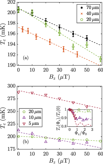
Figure 11. Transition temperature as a function of magnetic field for a series of unpatterned TESs with different bilayer side lengths. Each data point was calculated from a series of I(V) curves at varying bath temperature. (a) is for the larger devices whilst (b) is for the smaller ones. In (b) error bars are suppressed as they are smaller than the symbols used. Both figures show straight-line fits to the data as dashed lines. The lower figure inset shows  as a function of flux,
  . The fits in this inset are given by the weighted combination of equation (1) and a constant, representing the contributions from the superconducting and normal components of the current respectively.
Download figure:
Standard image High-resolution imageInterpretation of the measurements of  for smaller 5 µm and 10 µm TESs, shown in figure 11(b), in terms of flux-flow resistance is less compelling. This would be expected if
  [32]. The fluctuations in
  appear more closely related to the Fraunhofer patterns of the underlying Ic
as shown in the inset of figure 11(b). For the smaller TESs Jc
is reduced to close to zero at the expected minima.
appear more closely related to the Fraunhofer patterns of the underlying Ic
as shown in the inset of figure 11(b). For the smaller TESs Jc
is reduced to close to zero at the expected minima.
3.3.1. Effect of applied field on the TES bias current.
Figure 12 shows the relationship between the oscillations seen in transition temperature and bias current measured with increasing field. For the four 10 µm side length TESs studied, the change in  is plotted on the same axes as the normalised change in current
  . There is good agreement between the two sets of oscillations for all four TESs, suggesting that the same effects determine the period of oscillation of both critical current and bias current. For the TES with two partial bars, the broad minimum in
  at around 30–40 µT corresponds to a maximum in
  . The oscillations in
  in figure 6 also show a maximum around this region, suggesting that another physical process may be suppressing the maximum in
  .
.

Figure 12. Normalised changes  (black points) and
  (red points) as a function of magnetic field Bz
, for four 10 µm TESs with different numbers of normal metal bars. The blue number in the lower left corner of each subplot shows the number of partial normal metal bars on the TES.
(red points) as a function of magnetic field Bz
, for four 10 µm TESs with different numbers of normal metal bars. The blue number in the lower left corner of each subplot shows the number of partial normal metal bars on the TES.
Download figure:
Standard image High-resolution image3.3.2. Effect of magnetic field on TES responsivity.
In this section we consider the effect of magnetic fields on TES responsivity when used as a power detector. To do so it is first useful to consider how the calculation of the responsivity is modified in the presence of a magnetic field. Magnetic field affects the responsivity of a TES directly through its effect on the bias current (section 3.3.1).
TES are usually operated with voltage bias. However, the most-commonly used TES voltage-bias and readout circuit, as used here, is not an ideal voltage source [23]. In the standard circuit analysis, the combination of a low valued bias resistor Rb
(typically ∼ 1 mΩ) and any stray resistance Rstray are represented by a load resistance RL
. This means that the bias voltage of the TES Vb
changes if the TES current changes irrespective of details of the TES behaviour itself. For simplicity here we assume that the TES electrothermal parameters are near-ideal (α is large, β → 0) for all bias points. With these assumptions and for a TES used as a bolometer, the small-signal power-to-current responsivity of the TES in a small-signal analysis at an initial bias point is  [23]. In this analysis we identify
  for consistency with the complete small-signal analysis of [23]. If for example a magnetic field changes the bias current so that
  , the responsivity
  is also changed. Circuit analysis shows that
Note that for an ideal voltage bias  irrespective of
  . This responsivity is most-relevant for quantifying small-signal power detection in a bolometer, but similar considerations would apply for a calorimeter.
Figure 13(a) shows the responsivity as a function of magnetic field for a series of square TESs of 10 µm side length. The oscillations in responsivity are of similar magnitude for all of the TESs. Figure 13(b) shows the responsivity as a function of magnetic field for two 40 µm TESs. These larger devices display the smallest changes in responsivity with field, and the addition of partial normal metal bars further reduces sI
. Figure 13(b) also shows additional discontinuities near ± 3 µT and ± 15 µT that maybe indicative of phase-slip behaviour. These features were very reproducible as a function of applied field, with finer sampling with field, and even between cool-downs. The observation that larger TESs may display phase slip behaviour is consistent with the existing theoretical ideas [25, 30, 32]. These discontinuities in  were not observed in similar larger TESs with additional lateral bars.

Figure 13. Change in TES responsivity as a function of magnetic field through the bilayer. Measurements are for TESs with (a) 10 µm side length bilayers and (b) 40 µm side length bilayers, patterned with different numbers of normal metal bars. The bias currents at zero field are (a) plain: 4.52 µA, 1 bar: 3.91 µA, 2 bars: 4.06 µA and 3 bars: 3.27 µA and (b) plain: 2.85 µA and 3 bars: 2.32 µA. In (b) possible phase slips are indicated for the unpatterned TES.
Download figure:
Standard image High-resolution imageThe existing theoretical work does not, however, predict the result that the smallest TESs display the largest changes in current with flux, as these TESs have less magnetic flux threading them, which would imply that any changes in current with flux would be smaller. This suggests that there may be non-uniformities in the larger TESs, such as vortices, which reduce magnetic flux penetration and hence magnetic field sensitivity.
3.3.3. Directional dependence of bias and critical current on applied field.
To investigate the directional magnetic field dependence of the bias current of the TESs at fixed Vb
, the magnitude of the applied magnetic field was fixed and its direction varied. Using the full three-axis Helmholtz system, fixing  defines a sphere of fixed radius, which can be parametrised in terms of azimuthal and polar angles. In order to ensure efficient sampling, the increment of the azimuthal angle was fixed and the increment of the polar angle was varied to sample elements of equal area.
For the general field direction,

Equation (1) can be extended so that the critical current is [33]
As Bx
is parallel to the direction of current flow, the effect of  can be neglected. Figure 14 shows the model prediction of the change in critical current with the direction of a 50 µT applied field, for a 10 µm side length TES. The direction of the applied field is scaled by the resulting change in critical current, so for a TES that is equally sensitive to applied fields in all directions, the response surface would be spherical. The lobed response surface indicates that the thin film is most sensitive to magnetic fields applied perpendicular to the plane of the TES, as expected. The shading of the surface corresponds to the magnitude of the response. This model also predicts oscillations in the response, which can be seen both in the response surface and the cuts in the x − z and y − z planes shown underneath. The response is minimal when the applied field is in the x − y plane. The model suggests the general behaviour for Ib
of a real TES as a function of field orientation, although experimentally (compare for example figures 5 and 12) although we have already shown that the correlation is imperfect.
can be neglected. Figure 14 shows the model prediction of the change in critical current with the direction of a 50 µT applied field, for a 10 µm side length TES. The direction of the applied field is scaled by the resulting change in critical current, so for a TES that is equally sensitive to applied fields in all directions, the response surface would be spherical. The lobed response surface indicates that the thin film is most sensitive to magnetic fields applied perpendicular to the plane of the TES, as expected. The shading of the surface corresponds to the magnitude of the response. This model also predicts oscillations in the response, which can be seen both in the response surface and the cuts in the x − z and y − z planes shown underneath. The response is minimal when the applied field is in the x − y plane. The model suggests the general behaviour for Ib
of a real TES as a function of field orientation, although experimentally (compare for example figures 5 and 12) although we have already shown that the correlation is imperfect.
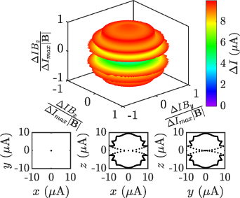
Figure 14. (Top) Change in critical current with direction of the magnetic field applied to a 10 µm × 10 µm TES thin film. In the plot, the direction of the field is scaled by the prediction of the change in critical current from equation (6), for an applied field of 50 µT. The shading corresponds to the magnitude of the response. The normal of the thin film is in the z direction. (Bottom) Cuts through the response surface in the x − y, x − z and y − z planes.
Download figure:
Standard image High-resolution imageFigure 15 shows the measured directional dependence of the change in bias current for 10 µm and 40 µm TESs either plain or with three lateral bars. The scans were taken at a temperature of 90 mK and a bias point of  , with a field magnitude of 20 µT. In each plot, the change in bias current at a given angle has been normalised by the maximum value recorded for all angles so as to emphasise the directional dependence. The colour of the points corresponds to the normalised total magnitude of response. Device geometry is indicated by the cartoon in the top right-hand corner of each plot. TES size increases across the columns of the figure and the number of bars down the rows.
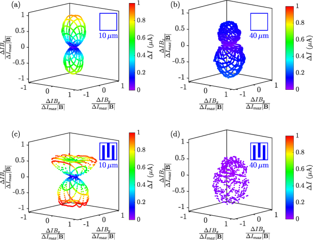
Figure 15. Change in TES bias current with direction of the magnetic field applied. The change in the measured TES bias current  is plotted as a function of normalised field direction for a fixed field
  = 20 µT. The blue diagrams in the top right corners of the plots indicate the dimensions and geometry of the bilayer. This figure shows plots for two unpatterned TESs with (a) a 10 µm and (b) a 40 µm side length bilayer, and for two TESs with three partial normal metal bars with (c) a 10 µm and (d) a 40 µm side length bilayer. These scans were taken at a temperature of 90 mK and a bias point of 50%
  . The colours of the points correspond to the magnitude of the current response.
Download figure:
Standard image High-resolution imageThe smaller unpatterned device shows the simplest directional behaviour: figure 15(a). This has a clean response surface, with a two-lobed form and with no visible oscillations (or ripples) with angle. The asymmetry in lobe sizes is most likely due to imperfect cancellation of the contribution from the earth's magnetic field and was seen for the other devices.
The larger unpatterned device, figure 15(b), displays more complicated behaviour. Ripples are visible in the response surface as the field angle is changed. This links to figure 13(a), which shows that for changes in magnetic field around and below 20 µT perpendicular to the plane of the thin film, SI
(hence Ib
) changes monotonically with field for an unpatterned TES but that a TES with three normal metal bars is operating close to a local maximum in SI
(minimum in Ib
). The relatively large oscillations in the response surface for this TES in an applied field of 20 µT arise from the local structure in  as the field direction is changed.
It can be seen by comparing the two rows of figure 15 that the addition of normal metal bars significantly reduces the directional magnetic field dependence of the TES about the z-axis. This is indicated by the broadening of the main response lobes, which are not described by the simple model in figure 14. In all cases the response in By and Bx is below our estimated experimental measurement error [29].
4. Discussion and conclusions
4.1. Summary of key observations
The key results of our measurements are summarised below, grouped by device parameter. For these Mo/Au TESs we observed different behaviour depending on whether the geometric side length was above or below ∼20 µm and we distinguish these two types of device as 'large' and 'small' respectively.
- 1.Field and temperature dependence of the critical current, Ic : the behaviour of Ic with field and temperature is important because of its expected influence on TES operating parameters, such as current in bias Ib . All devices showed some degree of Fraunhofer-like fluctuations in Ic with applied field Bz . The small, unpatterned, devices showed behaviour closest to that of an ideal short Josephson junction demonstrating well-defined zeroes of Ic with field. Increasing the side-length and adding partial lateral bars were both found to reduce the modulation depth of the pattern. Very different behaviour was observed in small patterned devices with odd and even numbers of bars that we attribute to the effect of self-field. In all cases the effective area of the device as determined from the change in Ic with applied flux was smaller than the physical area of the TES. The temperature dependence of Ic above Tc was well-described by the description of a SS'S weak-link above Tc given in Golubov et al [30] that was derived from the Usadel model. We found a characteristic length ξ = 450 ± 20 nm that was consistent with the calculated normal-state correlation length of the S' bilayer. The same conclusion was also reached by Sadleir et al [18]. Below Tc , followed the expected Ginzburg–Landau dependence for all TES sizes.Our measurements of Ic
were carried out at fixed bath temperature with . We would expect differences in the magnitude of Ic
under voltage-biased operation when , and where Joule heating raises the operating temperature of the TES above Tb
such that the actual TES operating temperature may indeed be lower than Tc
. However, the functional dependence of the behaviour should be similar.
- 2.Field dependence of the operating point of a voltage-biased TES with electrothermal feedback: all measurements were made on membrane suspended devices, so as to be representative of sensitive bolometric/calorimetric detectors for low incident powers or energies (and having low noise equivalent powers or high energy resolution respectively).Superconducting critical temperatures Tc were found to decrease with applied field by about 150 KT−1 and 500 KT−1 for large and small devices respectively. For larger TESs, the reduction in Tc could be modelled in terms of the effect of flux-flow resistance using a characteristic length ξ = 470 ± 20 nm, again consistent with ξ being the normal-state correlation length of the S' bilayer.The field dependence of Ib was found to be similar that of Ic , consistent with assumptions above. The Joule power in bias was found to be only weakly dependent on applied field, changing by ≈5% in a 50 µT field for a large TES.
- 3.Dependence of the operating current, Ib on field orientation: we measured the dependence of the change in Ib on field direction and found significantly reduced sensitivity to in-plane fields, as expected. We found that smaller TESs were most sensitive to applied fields. The addition of lateral bars also reduced the angular dependence.
- 4.TES power-to-current responsivity with applied field: TES power-to-current responsivity (change in current for a given change in input power) was shown to vary with field in all devices. Variations of order 10% with field were measured for small devices, with little reduction when bars were added. The variations were reduced in larger devices (∼ 2% for a 40 µm device) and the addition of three bars was found to suppress them nearly entirely. However, the larger device without lateral bars showed additional, reproducible, discontinuities in sensitivity (and bias current) not present in the small devices, which we attribute to the release or movement of pinned phase slip features.


4.2. Recommendations for application of TESs in a magnetic field
The measurements suggest routes towards optimal TES designs for future applications with respect to the effect of magnetic field.
We will primarily use the behaviour of the bias current  hence the power-to-current responsivity SI
to inform our recommendations, as it is most directly relevant to detector operation. In addition, the effects of the magnetic field on other parameters, like critical temperature and current, are primarily felt through their effect on this
hence the power-to-current responsivity SI
to inform our recommendations, as it is most directly relevant to detector operation. In addition, the effects of the magnetic field on other parameters, like critical temperature and current, are primarily felt through their effect on this  . In this paper we have not attempted to model the behaviour of
  in terms of, for example, the resistively shunted Josephson (RSJ) model [15, 19, 24] or a two-fluid model [34] but the key-point is that both require Tc
and Ic
as inputs in the modelling of Ib
.
in terms of, for example, the resistively shunted Josephson (RSJ) model [15, 19, 24] or a two-fluid model [34] but the key-point is that both require Tc
and Ic
as inputs in the modelling of Ib
.
Based on the observations reported our overall recommendations are listed below:
- Zero field should be the goal in all applications. B and changes in B should be minimized. But this may not be a realistic solution.
- The smallest TESs are least sensitive to changes in field near . See equation (1). Our measurements confirm this.
- TESs are less sensitive to changes in By and Bx as expected: see equation (1). Our measurements confirm this. Routing of cabling harnesses or positioning of apertures, for example, should consider this observation.

For operation in non-zero fields with fluctuations (that may occur or be unavoidable in applications) the comments depend on the magnitude of the fields but generally:
- Smaller TESs are more sensitive to changes in applied field see shown in figure 13.
- The larger TESs measured here were less susceptible to field (and variations).
- But for larger TESs we also observe discontinuities in Ib hence SI with Bz that would seriously compromise detector operation within a varying stray field.
- The addition of lateral normal metal bars further reduces the magnetic field sensitivity in Ib hence SI for larger TESs, and for these TESs no discontinuities in Ib were observed.

It is important to emphasise that these considerations do not represent an optimization for general TES design. Rather we expect the issues to be material, operating temperature and geometry dependent.
Acknowledgments
The authors would like to thank the Scottish Microelectronics Centre for growing the SiN/SiO2 membranes for the devices and for providing DRIE.
Data availability statement
The data cannot be made publicly available upon publication because they are not available in a format that is sufficiently accessible or reusable by other researchers. The data that support the findings of this study are available upon reasonable request from the authors.