
Abstract
We report measurements of the in-plane thermoelectric power (TEP) for an overdoped (OD) crystal of the single layer cuprate superconductor Tl2Ba2CuO (Tl2201) at several hole concentrations (p), from 300 or 400 K to below the superconducting transition temperature (Tc). For p = 0.192 and 0.220, small upturns in the TEP below 150 K are attributed to the presence of charge density waves (CDW) detected by resonant inelastic x-ray scattering studies. This suggests that measurement of the TEP could provide a simple and effective guide to the presence of a CDW. Over a certain temperature range, often strongly restricted by the CDW, the TEP is consistent with the Nordheim-Gorter rule and the T1 and T2 terms in the in-plane resistivity of similar crystals observed below 160 K. Two scenarios in which the T1 scattering term is uniform or non-uniform around the Fermi surface are discussed. As found previously by others, for uniform scattering the T1 terms give scattering rates (τ−1) at lower p that are somewhat larger than the Planckian value
  and fall to zero for heavily OD crystals. Near 160 K, τ−1 from the T2 terms corresponds to the Planckian value.
Export citation and abstract BibTeX RIS

Original content from this work may be used under the terms of the Creative Commons Attribution 4.0 license. Any further distribution of this work must maintain attribution to the author(s) and the title of the work, journal citation and DOI.
1. Introduction
Identifying the pairing mechanism in cuprate superconductors and the origin of the characteristic T-linear behavior of the in-plane electrical resistivity, are still controversial and unsolved questions that may turn out to be closely related. In this regard single crystals of Tl2Ba2CuO (Tl2201) are of great interest because their superconducting transition temperature (Tc
) can be progressively reduced from 90 K to zero by increasing the oxygen content, x, and they have lower in-plane residual resistivity than other cuprates such as La
(Tl2201) are of great interest because their superconducting transition temperature (Tc
) can be progressively reduced from 90 K to zero by increasing the oxygen content, x, and they have lower in-plane residual resistivity than other cuprates such as La Srx
CuO4 (LSCO) and Bi2Sr2CuO
Srx
CuO4 (LSCO) and Bi2Sr2CuO that can be overdoped (OD). Furthermore, any van Hove singularity is well away from the Fermi energy [1]. Quantum oscillation (QO) experiments, e.g. [2] show that heavily OD crystals with
  26 K have a large Fermi surface. There appears to be no work on strongly underdoped (UD) Tl2201 crystals, with difficulties caused, at least partly, by the volatility and toxicity of thallium compounds, but this does not affect our conclusions. Recently, charge density waves (CDW) have been detected below 150 K in a resonant inelastic x-ray scattering (RIXS) study of OD Tl2201 crystals [3] with higher Tc
. The question as to whether this can account for the unusual evolution of the Hall number as the hole doping (p) is reduced [1] is still being debated [4]. In this paper we report measurements of the in-plane thermoelectric power (TEP),
26 K have a large Fermi surface. There appears to be no work on strongly underdoped (UD) Tl2201 crystals, with difficulties caused, at least partly, by the volatility and toxicity of thallium compounds, but this does not affect our conclusions. Recently, charge density waves (CDW) have been detected below 150 K in a resonant inelastic x-ray scattering (RIXS) study of OD Tl2201 crystals [3] with higher Tc
. The question as to whether this can account for the unusual evolution of the Hall number as the hole doping (p) is reduced [1] is still being debated [4]. In this paper we report measurements of the in-plane thermoelectric power (TEP),  for a single crystal from the same preparation batch (October 2014) as in the RIXS and Hall effect work. We argue that the CDW gives a small but distinct upturn in
  below 150 K. This conclusion is reinforced by the observation of similar upturns in all polycrystalline samples [5] with
  K. Such data usually agree reasonably well with measurements of
  on single crystals.
We discuss in-plane electrical resistivity  data [1] for Tl2201 crystals and show that the TEP is consistent with the T1 and T2 terms in
  observed below 160 K and the Nordheim-Gorter (NG) rule. Corresponding scattering rates τ−1 are compared with the Planckian rate
  [6–8]. We estimate τ−1 at low T from
  and raise the question as to whether the residual low-T specific heat of OD Tl2201 [9] is caused by standard pair-breaking in a d-wave superconductor [10, 11] combined with a decrease in the strength of the pairing interaction [12, 13], or whether it is caused by the pairing interaction
  being sufficiently anisotropic so that some electrons are not paired. Namely if the T1 scattering term is much weaker on some parts of the Fermi surface does this imply that
  is much smaller there?
2. Results and analysis
2.1. Effect of CDW on the TEP
Above  the TEP of OD cuprates generally varies approximately as
  , where
  to
to  V K−1 and b changes from
  to
to  V K−1 as p is increased from 0.16, the value for maximum Tc
, to the upper edge of the superconducting dome [5] while for UD samples it is usually positive and much larger [5]. TEP data were taken in an earlier, independent research project before the RIXS studies, using the method described in the
V K−1 as p is increased from 0.16, the value for maximum Tc
, to the upper edge of the superconducting dome [5] while for UD samples it is usually positive and much larger [5]. TEP data were taken in an earlier, independent research project before the RIXS studies, using the method described in the  V K−1 below 50 K has been made for the Tc
= 29 K and 26.5 K data using the phosphor bronze results shown in the
V K−1 below 50 K has been made for the Tc
= 29 K and 26.5 K data using the phosphor bronze results shown in the
Figure 1(a) shows that the in-plane TEP  for the same Tl2201 crystal with Tc
values of 88 K and 67 K has a small upturn below ∼150 K, where there is also a clear change in the derivative
for the same Tl2201 crystal with Tc
values of 88 K and 67 K has a small upturn below ∼150 K, where there is also a clear change in the derivative  , as shown in figure 1(b), but there is no such effect for
  K. For
  K there is marginal evidence for a CDW with an onset near 40 K as indicated in figure 3. All this correlates well with RIXS measurements on Tl2201 crystals from the same preparation batch for which CDWs were detected for Tc
values of 56 K and 45 K but not for 22 K [3]. TEP data for Tc
= 88 K, on an expanded scale in figure 1(c), show a particularly clear anomaly near 145 K. The CDW onset temperature for Tc
= 45 K is 150 K as shown by the RIXS data on the right hand scale of figure 1(b) but unfortunately the onset temperature of 160 K shown in [3] for Tc
= 56 K is only an upper bound. Although better overlap of Tc
values would have been desirable it is very probable that the changes in
K there is marginal evidence for a CDW with an onset near 40 K as indicated in figure 3. All this correlates well with RIXS measurements on Tl2201 crystals from the same preparation batch for which CDWs were detected for Tc
values of 56 K and 45 K but not for 22 K [3]. TEP data for Tc
= 88 K, on an expanded scale in figure 1(c), show a particularly clear anomaly near 145 K. The CDW onset temperature for Tc
= 45 K is 150 K as shown by the RIXS data on the right hand scale of figure 1(b) but unfortunately the onset temperature of 160 K shown in [3] for Tc
= 56 K is only an upper bound. Although better overlap of Tc
values would have been desirable it is very probable that the changes in  and
and  near 150 K shown in figures 1(a)–(c) as well as at various temperatures for the polycrystalline data in [5] are caused by a CDW. This agreement is potentially useful because it shows that the TEP is a sensitive probe of the CDW and could be used to study its pressure dependence and possibly its magnetic-field dependence. Data for the OD88 crystal and the OD84 polycrystalline sample [5] show that the CDW is still present at lower p, which is a new finding.

Figure 1. (a) In-plane thermoelectric power  for the same Tl2201 crystal with 4 different Tc
values. p = 0.192, 0.220, 0.271 and 0.274 for Tc
= 88 K, 67 K, 29 K and 26.5 K respectively determined from the same modified formula used in [1] that accounts for the Fermi surface area obtained from quantum oscillation studies [2] for
for the same Tl2201 crystal with 4 different Tc
values. p = 0.192, 0.220, 0.271 and 0.274 for Tc
= 88 K, 67 K, 29 K and 26.5 K respectively determined from the same modified formula used in [1] that accounts for the Fermi surface area obtained from quantum oscillation studies [2] for  K. (b) Left-hand scale, corresponding derivative plots
  , and right-hand scale RIXS intensity vs
T for a crystal with Tc
= 45 K from [3]. The CDW causes a downturn in
, and right-hand scale RIXS intensity vs
T for a crystal with Tc
= 45 K from [3]. The CDW causes a downturn in  below 150 K, upturns at lower T are caused by the onset of superconductivity. Before forming the derivatives,
  and T data were smoothed over 5 points, typically ±10 K, 10 or 20 K above Tc
and ±4 K nearer Tc
. This reduced the scatter without causing other changes. (c) Inset, expanded view for Tc
= 88 K showing a clear anomaly at 145 K.
and T data were smoothed over 5 points, typically ±10 K, 10 or 20 K above Tc
and ±4 K nearer Tc
. This reduced the scatter without causing other changes. (c) Inset, expanded view for Tc
= 88 K showing a clear anomaly at 145 K.
Download figure:
Standard image High-resolution image2.2. T1 and T2 terms in the resistivity
Resistivity data [1] for five different crystals from the same preparation batch are shown in figure 2(a). As noted in [3] there appears to be no effect of the CDW on the in-plane resistivity  . This is unusual since other CDW materials do show resistivity anomalies, but it is reinforced by the derivative plots in figure 2(b). Although there is a change in slope of
  near 160 K, we do not believe that this is caused by a CDW. It is also present for the crystal with
  26.5 K and a crystal from another batch with
  17 K as well as for older data scanned in from [15].
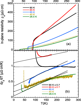
Figure 2. (a) In-plane resistivity data  for Tl2201 crystals from the same batch, taken from [1]. The crystal with Tc
= 85 K is probably underdoped [1] and not considered further here. The p values for the other crystals are 0.183, 0.227, 0.256 and 0.274 for Tc
= 90 K, 65 K, 40 K and 26.5 K respectively. (b) Corresponding derivative plots and straight lines expected when
for Tl2201 crystals from the same batch, taken from [1]. The crystal with Tc
= 85 K is probably underdoped [1] and not considered further here. The p values for the other crystals are 0.183, 0.227, 0.256 and 0.274 for Tc
= 90 K, 65 K, 40 K and 26.5 K respectively. (b) Corresponding derivative plots and straight lines expected when 
 . Data above 175 K for Tc
= 85 K were too noisy to give accurate derivatives. The straight lines show the results of least squares fits.
. Data above 175 K for Tc
= 85 K were too noisy to give accurate derivatives. The straight lines show the results of least squares fits.
Download figure:
Standard image High-resolution imageSuch derivative plots [16, 17] are a convenient way of applying the formula

because the range of fit is easily seen by inspection. They suggest that there are two distinct values for the T1 and T2 terms, below and above 160 K where both the slopes and the intercepts in figure 2(b) change. For the crystals with Tc
= 65 K, 40 K and 26.5 K, α1 and α2 were found from the intercepts at T = 0 and the slopes of the straight lines in figure 2(b), while the residual resistivity α0 was then found by fitting the data in figure 2(a) to a second order polynomial in which α1 and α2 were fixed. The coefficients α are given in table 1. (A small correction for a measurement offset of  below Tc
has been included where appropriate). Here we focus on the values below 160 K, expecting them to be more closely related to superconductivity. The coefficient α1 is presently of great interest because of the suggestion that the Planckian scattering rate
below Tc
has been included where appropriate). Here we focus on the values below 160 K, expecting them to be more closely related to superconductivity. The coefficient α1 is presently of great interest because of the suggestion that the Planckian scattering rate  [6] is the maximum allowed for any material [8], and that it is an important intrinsic property of superconducting cuprates [7] and many other correlated metals [8]. The Drude formula for the in-plane conductivity of an isotropic cylindrical Fermi surface,
  , which is a reasonable first approximation for Tl2201, shows that
  1
1  corresponds to
  , if the carrier density n = 1.3 holes per unit cell and
  . Although this value of
  has been measured by QO only for OD Tl2201 [2], specific heat data [9] show that it only varies weakly with p. So
  0.3
0.3  in figure 2(b) corresponds to
  . For crystals with
  50 K,
50 K,  falls below this value because, as found previously [16, 17], the size of the T1 term falls linearly to zero as p approaches the edge of the superconducting dome. This could be an indication that the anomalous scattering becomes confined to certain parts of the Fermi surface, in contrast to the results for some other cuprates [7]. The value of α0 for Tc
= 26.5 K in table 1, gives
falls below this value because, as found previously [16, 17], the size of the T1 term falls linearly to zero as p approaches the edge of the superconducting dome. This could be an indication that the anomalous scattering becomes confined to certain parts of the Fermi surface, in contrast to the results for some other cuprates [7]. The value of α0 for Tc
= 26.5 K in table 1, gives  K and for a Fermi velocity
  cm s−1, a mean free path of 68 nm. Specific heat data for Tl2201 [9] show a large residual linear term which increases as p approaches the edge of the superconducting dome, as expected for a d-wave superconductor when
  becomes comparable with Tc
.
becomes comparable with Tc
.
Table 1. Values of α given by the straight lines below 160 K in figure 2(b) plus a constrained fit to the data in figure 2(a) (see text), i.e.  . The carrier mean free path (mfp) is obtained from α0.
  values are from figure 1(a). S0, S1 and S2 are from fits to equation (2), but cannot be determined independently (see text). The errors in α values are
  from geometrical uncertainties.
| Tc | α0 | α1 |

| mfp |

| S
| S
| S
|
|---|---|---|---|---|---|---|---|---|
| (K) | ( ) ) | ( ) ) | ( ) K−2) ) K−2) | (nm) | (K) | (µV K−2) | (µV K−2) | (µV K−2) |
| 90 |

| 1.37 | 0.125 | — | 88 | 0.132 |

| — |
| 65 | 6.3 | 0.313 | 1.82 | 65 | 67 | 0.128 | — |

|
| 40 | 6.9 | 0.17 | 1.34 | 60 | — | — | — | — |
| 26.5 | 6.0 | 0.053 | 1.6 | 68 | 26.5 | 0.016 | — |

|
Previously [16] the deviations from a straight line above 160 K for the three most overdoped crystals in figure 2(b). were interpreted in terms of a parallel conducting channel and the maximum resistivity of 1800  obtained when the carrier mean free path is equal to the in-plane lattice spacing a. However they are still clearly visible for the two most overdoped crystals in figure 2(a) that have resistivities as low as 60
  at 160 K and as mentioned already for another crystal from a different preparation batch with
  K. Therefore we have no clear interpretation of this effect. It is worth noting that α2 is rather insensitive to p as also shown in [16]. At 160 K it corresponds to a T2 term in the resistivity of 40
  and, making the same assumptions as before, a scattering rate
  , the Planck condition [6]. This observation could have ramifications for interpretations of the T1 term arising from the Planck condition. Perhaps
  might cause the deviations from linearity in figure 2(b) above 160 K. Alternatively the deviations might be connected with the effect of lattice vibrations on electron–electron Umklapp scattering. Electron–electron scattering is rarely studied up to such high temperatures. It is known that the Debye–Waller factor, which reduces the intensity of x-ray diffraction lines, causes the energy gap of semiconductors such as Si to fall as T is increased. It is possible that Umklapp scattering between Brillouin zones is reduced by a similar T-dependent factor that becomes more significant as the amplitude of the lattice vibrations increases.
Data for all hole-doped cuprates clearly show that the curvature of in-plane  plots increases on the OD side. It is widely accepted that there is a crossover line on the T − p phase diagram [18], which although ill-defined, increases linearly with p from zero for
  . It can be interpreted as a coherence temperature
  for the charged carriers and when
  the T2 term dominates. The results for
  160 K in figure 2(b) and table 1 are qualitatively consistent this is because α1 falls with p while α2 stays constant. For
  160 K this requires the slope of
  to become constant which is the case above 200 K for
  30 K [16] and for data in [15] above 250 K for several Tc
values between 0 and 80 K. It is puzzling that this does not hold for Tc
= 65 K in figure 2(b) suggesting that more data are needed to clarify this point. We note that there can be complications from Cu ions on the Tl sites affecting p [14] as well as time dependent changes in Tc
when a Tl2201 crystal is held at room temperature [19] that were also seen in our TEP data for Tc
= 26.5 K after one month at room temperature after the first anneal.
30 K [16] and for data in [15] above 250 K for several Tc
values between 0 and 80 K. It is puzzling that this does not hold for Tc
= 65 K in figure 2(b) suggesting that more data are needed to clarify this point. We note that there can be complications from Cu ions on the Tl sites affecting p [14] as well as time dependent changes in Tc
when a Tl2201 crystal is held at room temperature [19] that were also seen in our TEP data for Tc
= 26.5 K after one month at room temperature after the first anneal.
2.3. Pair breaking vs 'Not-pairing'
There seems to be two possible ways of explaining the variation of α1 and Tc
with p, which we will refer to as scenarios A and B. The more standard one, scenario A, based on the usual d-wave form for the pairing interaction, 

 , has been thoroughly analyzed and discussed in [10, 11] and related papers where the importance of small angle scattering was emphasized. Here Tc
falls as p is increased because the pairing interaction falls [12, 13] and hence
, has been thoroughly analyzed and discussed in [10, 11] and related papers where the importance of small angle scattering was emphasized. Here Tc
falls as p is increased because the pairing interaction falls [12, 13] and hence  where Δ is the superconducting energy gap, is larger. The theory is very similar to that used to understand the effect of magnetic impurities in classical superconductors. Experimental evidence for the relation between Tc
and ρres is summarized in [20] for both UD and OD cuprates. A second, less conventional one, scenario B, involves a different variation of the pairing interaction around the Fermi surface and is considered later. Scenario A could be referred to as 'pair-breaking' and B as ʼnot-pairing'. For our data set, the values of α0 for the OD65, OD40 and OD26 crystals in table 1 are very close to that in [11] for their OD25 crystal measured using microwaves.
where Δ is the superconducting energy gap, is larger. The theory is very similar to that used to understand the effect of magnetic impurities in classical superconductors. Experimental evidence for the relation between Tc
and ρres is summarized in [20] for both UD and OD cuprates. A second, less conventional one, scenario B, involves a different variation of the pairing interaction around the Fermi surface and is considered later. Scenario A could be referred to as 'pair-breaking' and B as ʼnot-pairing'. For our data set, the values of α0 for the OD65, OD40 and OD26 crystals in table 1 are very close to that in [11] for their OD25 crystal measured using microwaves.
2.4. NG analysis
In standard transport theory, when there are two or more independent scattering mechanisms, for example electron-impurity and electron-phonon scattering, giving contributions ρ0 and ρ1 to the resistivity, the total resistivity  , which is known as Matthiessen's rule (MR). For ordinary metallic alloys MR is a good first approximation although there are systematic deviations from MR that are well-documented [21]. There is considerable experimental evidence for Zn-doped YBCO and LSCO that MR applies to the T—independent impurity scattering and the T1 scattering terms in the cuprates [22–24]. The equivalent way of calculating the TEP is via the NG [25] rule:

where S0 and S1 etc are the corresponding contributions to the TEP. If the electron diffusion TEP is dominant, and there are no small energy scales, these will be proportional to T, but with different signs and magnitudes governed by the energy dependence of the particular scattering mechanism. As shown in table 1 the Tc values in figure 1 are close enough to some of those in figure 2(a) so the coefficients α can be used directly to calculate the TEP via equation (2).
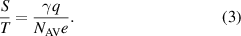
For  67 K the parameters S0, S1, and S2, all assumed to be proportional to T, were found by fitting the TEP data in figure 1(a) to equation (2). The range of fit was very limited, to below 200 K because of deviations from equation (1) at higher T and for the two higher Tc
values to above 150 K, because of the onset of the CDW. Partly as a result of this, only the parameter S2 representing the contribution to the TEP from the T2 resistivity term is well-defined, although the term S0 from impurity scattering must be positive. This procedure did not work for
67 K the parameters S0, S1, and S2, all assumed to be proportional to T, were found by fitting the TEP data in figure 1(a) to equation (2). The range of fit was very limited, to below 200 K because of deviations from equation (1) at higher T and for the two higher Tc
values to above 150 K, because of the onset of the CDW. Partly as a result of this, only the parameter S2 representing the contribution to the TEP from the T2 resistivity term is well-defined, although the term S0 from impurity scattering must be positive. This procedure did not work for  90 K where it gave the very small value of α2 shown in table 1 and a negative value for α0. For this crystal we therefore set
  , the average for the other three Tc
values, giving the values of S1 and S0 shown in table 1. For Tc
= 88 K and 67 K S0 must be at least 0.1µV K−2 which is unexpectedly large. In figure 3 it can be seen that the calculated SNG
curves for Tc
= 67 K and 26.5 K, agree well with the data giving
, the average for the other three Tc
values, giving the values of S1 and S0 shown in table 1. For Tc
= 88 K and 67 K S0 must be at least 0.1µV K−2 which is unexpectedly large. In figure 3 it can be seen that the calculated SNG
curves for Tc
= 67 K and 26.5 K, agree well with the data giving  V K−1, of the same sign and approximately 3 times larger than S1 for Tc
= 90 K. We can therefore conclude that the energy dependence of the T1 scattering term has the same sign as that of the T2 term, which is generally attributed to electron–electron scattering, but is significantly smaller. Measurements in which the superconductivity is suppressed by a magnetic field and on crystals with different residual resistivity, possibly controlled by doping with in-plane impurities such as Zn, would provide a further test of this picture. The magnitude of S2 is discussed below. Because of momentum conservation the electron–electron scattering contribution to
V K−1, of the same sign and approximately 3 times larger than S1 for Tc
= 90 K. We can therefore conclude that the energy dependence of the T1 scattering term has the same sign as that of the T2 term, which is generally attributed to electron–electron scattering, but is significantly smaller. Measurements in which the superconductivity is suppressed by a magnetic field and on crystals with different residual resistivity, possibly controlled by doping with in-plane impurities such as Zn, would provide a further test of this picture. The magnitude of S2 is discussed below. Because of momentum conservation the electron–electron scattering contribution to  usually depends on Umklapp scattering processes which will generally tend to be stronger for larger energies. This implies that for electrons, the electron–electron scattering term S2 will be positive and for holes it will be negative in agreement with experiment for Tl2201. Within this NG picture the changes in TEP below 160 K in figure 1(a) as p is increased are caused by the increase in the ratio
  with doping p and the fact that
  is larger than
  .
.
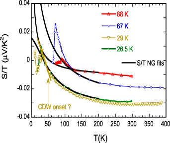
Figure 3.
 vs
T for Tc
= 88 K, 67 K, 29 K and 26.5 K together with fits to equation (2) for
vs
T for Tc
= 88 K, 67 K, 29 K and 26.5 K together with fits to equation (2) for  88 K, 67 K and 26.5 K, solid lines, with parameters given in table 1.
Download figure:
Standard image High-resolution image2.5. Possible anisotropy around the Fermi surface, scenario B
In the previous sections it was assumed implicitly that the T1 and T2 scattering rates do not vary appreciably around the Fermi surface, so that their contributions to  can be added in the same way as for electron-phonon and electron-impurity scattering. This is only approximate because there is experimental evidence from angle-dependent magnetoresistance (ADMR) of the c-axis resistivity [26] that for crystals with Tc
= 20 K, 17 K and 15 K, the anisotropy, (the parameter α in [26]) increases from 15
can be added in the same way as for electron-phonon and electron-impurity scattering. This is only approximate because there is experimental evidence from angle-dependent magnetoresistance (ADMR) of the c-axis resistivity [26] that for crystals with Tc
= 20 K, 17 K and 15 K, the anisotropy, (the parameter α in [26]) increases from 15 at 20 K to 40
 at 110 K. Recently, new short-range CDW signals have been identified in RIXS studies of many cuprate families [27]. These are present for a wide range of p, including the 'strange metal' region, p > 0.19, that is relevant for Tl2201 although such short range signals have not yet been observed for Tl2201. They are short-ranged in real space, and therefore broader in reciprocal space and are visible to higher T than the CDWs that have reasonably well-defined, often incommensurate, wave vectors
  . It has been argued that [28] that scattering from these short-range charge density fluctuations (CDF) are responsible for the T1 term in
  and because the CDF have a wide range of
  vectors they would indeed give isotropic scattering. So if CDF could be observed in Tl2201 crystals a good experimental test of this approach would be to compare their intensities with the size of the T1 terms in
  for different values of p.
Calculations by Rice et al [29] are more consistent with scenario B. These are based on the theory of Yang et al [30] and show that Umklapp scattering between hot spots gives rise to a T1 scattering rate in a very limited region of  -space and a corresponding T1 term in
  . They are not based on the usual Boltzmann transport equation. Somewhat paradoxically, in an earlier paper using the variational principle [31] to solve the Boltzmann equation, Hlubina and Rice [32] showed that the T2 term will dominate, although of course at low enough T any non-zero T1 term must become larger than a term going as T2. In this scenario
  at or near the hot spots is likely to be close to the Planck value because for
  0.19 where any T2 term is very small, as shown for example in table 1,
  is somewhat larger than the Planck value. It may be possible to distinguish between scenarios A and B by measuring the resistivity and London penetration depth on several crystals with similar Tc
values. Scenario B provides a more direct link between the T1 term and the superfluid density, emphasized recently in [17], than scenario A. However unlike scenario A it would not necessarily account for MR, the NG rule or the ADMR results. One possible test would be to see if either scenario can account for the 'vertical scaling' of the electronic specific heat [33] in applied magnetic fields.
is somewhat larger than the Planck value. It may be possible to distinguish between scenarios A and B by measuring the resistivity and London penetration depth on several crystals with similar Tc
values. Scenario B provides a more direct link between the T1 term and the superfluid density, emphasized recently in [17], than scenario A. However unlike scenario A it would not necessarily account for MR, the NG rule or the ADMR results. One possible test would be to see if either scenario can account for the 'vertical scaling' of the electronic specific heat [33] in applied magnetic fields.
2.6. Comparison with the TEP of other correlated electron materials
The low T TEP of many correlated electron materials, including some where the T2 term in  is dominant, has been shown [34] to obey the following simple empirical formula:
Here γ is the Sommerfeld coefficient, NAV Avogadro's number and e the magnitude of the electronic charge. The Faraday number  Coulombs/mole. For the simple case of free electron dispersion and 1 electron per formula unit,
  so taking
  [9] gives
  V K−1 at 160 K, the end of the linear regions in figure 2(b). This will be reduced by a factor
  by the larger carrier concentration and by a factor 2/3 for a constant carrier mean free path [34] giving
  V K−1 at 160 K. The value of
  V K−1 in table 1 gives a TEP of
  V K−1 at 160 K. So the T2 electron–electron scattering term in our TEP data for Tl2201 crystals agrees well with findings [34] for many other correlated electron materials, while the contribution from the T1 term is approximately a factor 3 smaller.
3. Summary
We have argued that the presence of CDWs can be seen in the in-plane TEP of Tl2201 crystals and in earlier data [5] for polycrystalline samples where the measured TEP is very similar to  for similar values of p. The NG rule seems to provide an adequate description of the TEP contributions arising from the T1 and T2 terms in the in-plane electrical resistivity. The magnitude of the TEP contribution from the T2 term agrees with that for other correlated electron conductors [34] while the contribution from the T1 term is
  times smaller. If the T1 term were truly anomalous one might perhaps have expected a larger difference. Within a simple cylindrical Fermi surface approximation, taking into account the known value of
  , the T1 terms for the crystals with Tc
of 40 K and 26.5 K correspond to scattering rates
, the T1 terms for the crystals with Tc
of 40 K and 26.5 K correspond to scattering rates  that are significantly smaller than the Planckian value
  , possibly indicating that τ is anisotropic. A strongly anisotropic scattering rate could provide a direct way of understanding the apparent correlation between the magnitude of the T1 term and the superfluid density emphasized recently [17], namely only those carriers with a T1 scattering rate would be paired. But there could be difficulties in accounting for MR, the NG rule and the ADMR work which suggests a small anisotropy at low T [26]. Also an extremely strong variation in
  might not be consistent with d-wave behavior. Somewhat unexpectedly, near 160 K, the T2 term corresponds to a scattering rate
  for all values of the hole concentration.
Acknowledgments
This work was funded by the EPSRC (U.K.) Grant Number EP/K016709/1. We are grateful to Prof. N E Hussey for helpful comments on the first draft of the manuscript.
Data availability statement
All data that support the findings of this study are included within the article (and any supplementary files).
Appendix:
A.1. Method used for TEP
The basic method used for the TEP is similar to that originally used for sintered polycrystalline bars in [5], but because of the small size of the crystals, and the fact that thicker crystals or thin films on a crystalline substrate have high thermal conductance, Au reference wires and Chromel wires forming two differential thermocouples are attached to Au pads on the ends of the crystal as shown in the photograph in figure A1. These wires extend for a few centimeters before being soldered to Cu wires heat sunk to a high thermal conductivity Cu block. A temperature difference ( K) is produced by alternately heating two sapphire blocks to which the thermocouple wires are attached with General Electric GE-7031 low temperature varnish and the Seebeck coefficient of the sample Ssample is given by eliminating
  from the equations:


Here the voltages across the Au wires,  and the Chromel wires,
  are measured using a Keithley Instruments digital nanovoltmeter and a home-built nanovolt amplifier respectively, and their ratio obtained by making a least squares linear fit to a plot of
  vs
vs
 for
for  and two points with
  . SCh is the Seebeck coefficient of Chromel taken from published standards and shown in figure A2. The same reel of
  m diameter Au wire was always used and SAu, also shown in figure A2 was obtained by measuring a strip of pure Pb which has a low TEP [35].
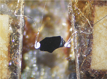
Figure A1. Photo of the 1.5 mm long Tl2201 crystal used for TEP measurements. 50 µm diameter Au wires and 25 µm diameter Chromel wires are spot-welded together to form differential thermocouples that are attached to Au pads on the crystal with DuPont 4929 N silver paint. The Au wires are heat sunk to sapphire plates with General Electric GE-7031 low temperature varnish.
Download figure:
Standard image High-resolution image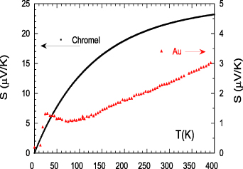
Figure A2. Thermopower of Chromel and Au wires used in the present work.
Download figure:
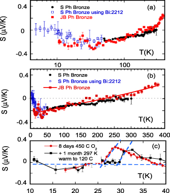
Standard image High-resolution imageIn the past further checks have been made by measuring a superconducting cuprate, Bi2212 with  90 K, and a piece of 127 µm diameter phosphor bronze alloy wire purchased from Lake Shore Cryotronics which has a conveniently low TEP. In the present work a piece of the same wire was measured again and compared with earlier data, as shown in figures A3(a) and (b). Small changes in the TEP of Au can be induced by bending (cold working) the wire which will change the phonon drag component and the electron diffusion component from any Fe impurities. Measuring the phosphor bronze wire is a convenient method of correcting for such changes. Figure A3(c) shows the TEP data from figure 1(a) after making a small correction of
  V K−1 corresponding to the difference in the TEP of the phosphor bronze wire at low T in earlier and more recent measurements shown in figure A3(a). It can be seen that Tc
rises from
V K−1 corresponding to the difference in the TEP of the phosphor bronze wire at low T in earlier and more recent measurements shown in figure A3(a). It can be seen that Tc
rises from  to
to  K after one month at room temperature after the first anneal.
Figure A3. (a) and (b) TEP of Lake Shore Cryotronics phosphor bronze alloy wire on logarithmic and linear temperature scales respectively. The most recent data labeled JB Ph Bronze is compared with earlier measurements, including one data set where the superconducting Bi2212 sample had zero TEP below 85 K. (c) Low T data for the Tl2201 crystal after making a small correction of  V K−1, given by the data in (a). The dashed lines show how Tc
values of 26 K and 29 K are determined.
V K−1, given by the data in (a). The dashed lines show how Tc
values of 26 K and 29 K are determined.
Download figure:
Standard image High-resolution image
Supplementary data (1.1 MB PDF)