
Abstract
We propose a refractometric sensor based on hollow silicon Mie resonators of a toroidal magnetic dipole mode. This mode has a pair of antiparallel electric dipoles perpendicular to the silica substrate; thus, the radiation of the mode is suppressed, resulting in an ultra-narrow reflection peak linewidth of 0.35 nm. In addition, the hollow structure enhances the interaction between the enhanced electric field and the surrounding medium, thus improving the sensitivity. The proposed Mie resonators achieve a sensitivity of 486 nm RIU−1 and a figure of merit up to 1389 RIU−1, which are ideal for refractometric sensing.
Export citation and abstract BibTeX RIS

Content from this work may be used under the terms of the Creative Commons Attribution 4.0 license. Any further distribution of this work must maintain attribution to the author(s) and the title of the work, journal citation and DOI.
Metasurfaces refer to thin films with engineered optical properties consisting of subwavelength-sized structures. 1–5) Refractometric sensors based on metasurfaces are of interest due to their high sensitivity S, low cost, simple measurement setup, and real-time monitoring. Plasmonic metasurfaces based on localized surface plasmon resonance can achieve high S 6) but have a low figure of merit (FOM) (e.g. less than 5 RIU−1) 7) due to high ohmic losses in the visible and NIR regions that produce broad resonance peaks.
Silicon metasurfaces have great potential for realizing refractometric sensors with high FOM due to very low material loss. Silicon metasurfaces support Mie-type resonant modes, such as electric dipole (ED), magnetic dipole (MD), 8) electric quadrupole (EQ), magnetic quadrupole (MQ), 9) and toroidal dipole (TD) modes. 10,11) Cylindrical Mie resonators based on ED and MD modes have low S values 12) because the enhanced electric field of these two modes is confined in the Mie resonators, making their peak wavelengths less sensitive to changes in the surrounding medium.
To achieve higher S values, the enhanced electric field of the resonant modes should extend more beyond the Mie resonators. By changing the Mie resonators from cylinders to nanodisks, the S values of the Mie resonators based on ED and MD modes reach 227 nm RIU−1 (RIU: refractive index unit) 13) and 385 nm RIU−1, 14) respectively. The S value of the cylindrical Mie resonators based on TD mode reaches as high as 470 nm RIU−1. 15) Despite the high S values of these Mie resonators, they do not obtain narrow peak linewidths, and thus the FOM still needs to be improved.
In this paper, we propose hollow silicon Mie resonators based on the toroidal MD (TMD) mode. We propose that the S value can be improved, and radiation can be suppressed by changing the size of holes in the Mie resonators. The S value of the proposed hollow Mie resonators is as high as 486 nm RIU−1. The full width at half maximum (FWHM) of the reflection peak is narrowed down to 0.35 nm, resulting in a FOM of up to 1389 RIU−1.
We first study a cuboid Mie resonator of width w and height h suspended in air, as shown in Fig. 1(a). We use a commercial 3D simulator (ANSYS Lumerical FDTD) based on the finite-difference time-domain (FDTD) method to calculate the scattering cross-section of the Mie resonator, where the scattering coefficient is equal to the ratio of the scattering cross-section to the geometric cross-section. Subsequently, we used COMSOL to study the multipole response of the Mie resonator. Figure 1(b) shows that the scattering coefficient calculated by Lumerical FDTD (black solid line) and COMSOL (grey dashed line) are in good agreement. We confirm that the peaks of the ED and MD modes are located at 2500 nm and 2700 nm, respectively (see Supplementary S1 for the multipole decomposition and field distribution of hollow Mie resonators). Higher-order modes, such as the EQ, MQ, electric octupole, and magnetic octupole modes, have weak responses and are therefore not discussed further.
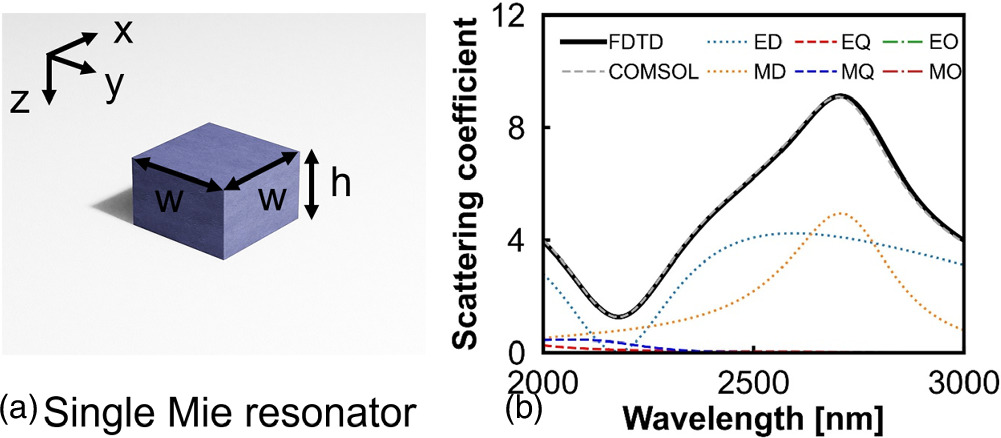
Fig. 1. (a) Schematic of a cuboid silicon Mie resonator in air. (b) Scattering coefficient of a cuboid Mie resonator of w = 800 nm and h = 500 nm. Incident light propagates in the z-direction.
Download figure:
Standard image High-resolution imageSubsequently, we study the collective response of Mie resonator arrays. Figure 2(a) shows a schematic of the Mie resonator array (see Supplementary S2 for the technical process of fabrication). The Mie resonators are arranged on a silica substrate with a period p. The width of the holes in the Mie resonators is w1. Material losses in undoped silicon and silica are negligible in the wavelength range of this study. The surrounding medium is assumed to be water, which will slightly attenuate the infrared light. 16) For simplicity, in studying the refractometric sensing performance of the proposed hollow Mie resonators, we assume that all the liquids used are lossless. In practice, the wavelength of the resonant modes should be adjusted to ensure that the reflection peaks can be measured. Figure 2(b) shows a reflection spectral map of the hollow Mie resonator arrays with w1 from 0 to 750 nm. At w1 = 0, the peak wavelengths of the ED and MD modes are almost the same. The destructive interference of the electric field scattered by the EDs and MDs in the backward direction leads to the suppressed reflection at 2277 nm. The peak of the ED mode has a larger blue shift compared to that of the MD mode as w1 increases. This is because the ED mode originates from the collective polarization of the material in the presence of the electric field of the incident light. In contrast, the MD mode, which is generated by a circular electric displacement current loop, requires enough retardation of the incident electric field by the Mie resonator, and thus the peak wavelength of the MD mode is more sensitive to changes in h. 8) With increasing w1, the peak of the ED mode disappears. Our study focuses on the MD mode because the reflection peak of the MD mode changes regularly with w1. In addition to the wavelength, the peak linewidth of the MD mode also changes with w1. This is because the radiative MD mode gradually transforms into non-radiative TMD mode as w1 increases. To verify our conjecture, we study the electric and magnetic field distributions of the MD (or TMD) mode at w1 = 150 nm, 450 nm, and 750 nm, as shown in Fig. 3. Figure 2(c) shows a schematic of the TMD in a hollow Mie resonator, aiding in the comprehension of the field distributions shown in Fig. 3 (see Supplementary S3 for more discussion of the TMD mode).

Fig. 2. (a) Schematic of a hollow Mie resonator array immersed in liquid. (b) Reflection spectral map of the Mie resonators with w = 800 nm, h = 500 nm, w1 = 0–750 nm, and p = 1000 nm. The n of the surrounding medium is set to 1.31 (water). The electric field of the incident light is x-polarized. (c) Schematic of the TMD in a hollow Mie resonator.
Download figure:
Standard image High-resolution image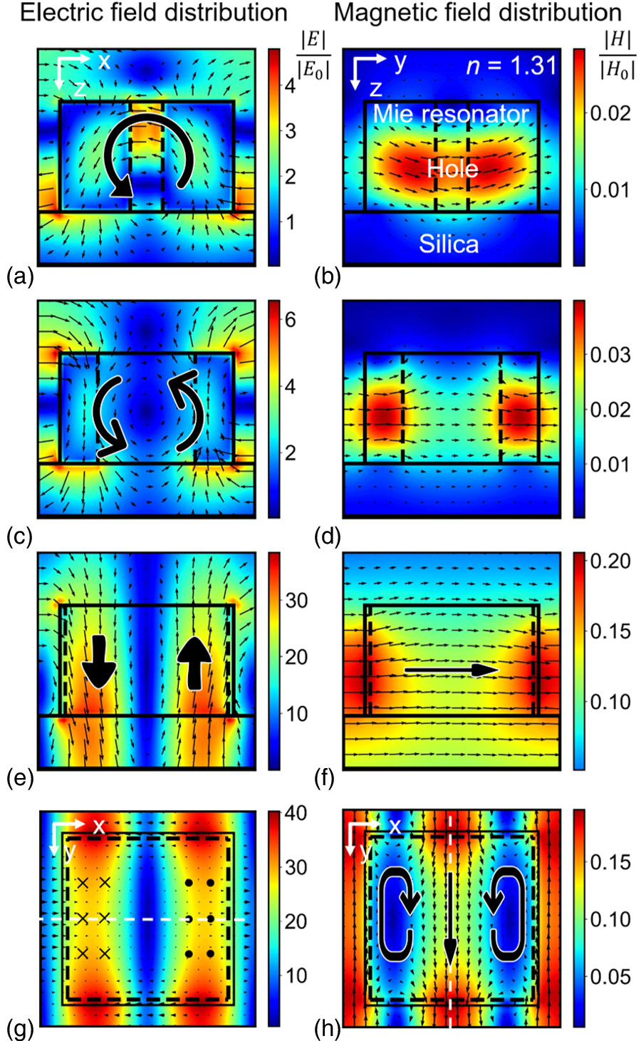
Fig. 3. (a) Electric and (b) magnetic field distributions at 2208 nm for the Mie resonators with w1 = 150 nm. (c) Electric and (d) magnetic field distributions at 2003 nm for the Mie resonators with w1 = 450 nm. (e) Electric and (f) magnetic field distributions at 1465 nm for the Mie resonators with w1 = 750 nm. (g) Electric and (h) magnetic field distributions in the x–y plane at 1465 nm. The field distributions are normalized to the amplitudes of the incident fields E0 and H0. The electric field of the incident light is polarized along the x-direction.
Download figure:
Standard image High-resolution imageIn Figs. 3(a) and 3(b), we can see a distinct circular electric displacement current loop and an induced MD for the Mie resonator of w1 = 150 nm, which are common field distributions for the MD mode. 14) As the w1 increases to 450 nm, the electric field distribution of the MD mode is more like a combination of a circular electric displacement current loop and a pair of antiparallel EDs perpendicular to the silica substrate, as shown in Fig. 3(c). From Fig. 3(d), we can still see the MD. The transformation of the electric field is due to the strong field confinement provided by the high n of silicon (n = 3.47). The increase of w1 leads to the decrease of the area of silicon in the x-z plane, which compresses the electric field. Figures 3(e) to 3(h) show the field distributions of the TMD mode when the w1 is equal to 750 nm. The circularly distributed magnetic field [Fig. 3(h)] induces the antiparallel EDs [Figs. 3(e) and 3(g)] perpendicular to the substrate, and the TMD [Figs 3(f) and 3(h)] is induced by the antiparallel EDs. 11,17) It is important to note that although the TMD mode has the same main features in the hollow Mie resonators and split nanodisks, 11) the field distributions are slightly different. The limited volume of silicon in the hollow Mie resonators does not allow for effective field confinement in silicon. Hence, the enhanced field extends mainly into the surrounding medium, making this structure more affected by the surrounding medium and thus more suitable for sensing. The TMD mode exhibits ∼40-fold enhancement in local electric field amplitude compared to the incident electric field, signifying longer resonance duration and lower radiation loss.
Figure 4(a) shows the FWHM of the MD (and TMD) mode peaks at different w1. The peaks of the ED and MD modes overlap at w1 = 150 nm; therefore, the peak FWHM plot of the MD mode starts at w1 = 250 nm in steps of 100 nm. At w1 = 250 nm, the FWHM of the peak of the MD mode is 176 nm. The FHWM decreases with increasing w1. Surprisingly, at w1 = 750 nm, the FWHM of the TMD mode is as low as 0.41 nm. Two factors contribute to the non-radiative characteristics of the TMD mode. First, the coherent oscillation of the TMD mode in the array causes light scattering in the Mie resonator plane (x–y plane) to occur only at the edges of the array. 18) The size of the Mie resonator array in the simulations is infinite, so the light radiation in the x–y plane is negligible. We mainly consider light scattering in the z-direction, i.e. the direction of the incident light. Radiation in the z-direction is effectively suppressed because the induced antiparallel EDs are aligned with the z-axis. 11) As a result, the TMD mode is a non-radiative mode for the hollow Mie resonators with w1 = 750 nm. Figure 4(b) shows the S values of the MD (and TMD) mode for different w1. The S value is defined as S = Δλ/Δn, where Δλ is the change of the reflection peak wavelength of the MD mode when the n of the surrounding medium changes from 1.31 (water) 16) to 1.345 (ethanol). 19) The main trend is that the S value of the MD (and TMD) mode increases with increasing w1. This is because the enhanced electric field extends outside the hollow Mie resonators where w1 is larger, as shown in Fig. 3, and thus the peak wavelength of the MD (and TMD) mode is more sensitive to the change of the surrounding medium. At w1 = 750 nm, the hollow Mie resonator achieves an S value of as high as 440 nm RIU−1. Although the S value at w1 = 650 nm (445 nm RIU−1) is slightly greater than that at w1 = 750 nm, a FOM of up to 1069.4 RIU−1 can be achieved due to the narrow peak linewidth at w1 = 750 nm.
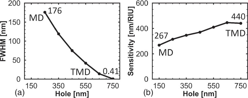
Fig. 4. (a) FWHM and (b) S values of the hollow Mie resonator arrays with w1 = 150–750 nm in steps of 100 nm.
Download figure:
Standard image High-resolution imageFigure 5(a) shows the reflection spectra of the hollow Mie resonator array with w1 = 750 nm at different n. To further improve the S value and FOM, the silica substrate can be etched. According to the electric field distribution in Fig. 3(e), part of the enhanced electric field appears in the silica substrate. After etching, part of the enhanced electric field in the silica substrate can be exposed to the surrounding medium. Hence, the S value can be improved, as shown in Fig. 5(b). We set the etching thickness of silica to 100 nm. If a larger value, such as 200 nm, is used, the peak wavelength of the TMD mode is close to the wavelength of the Rayleigh anomaly, which will excite lattice resonances with lower S values. 14) By etching 100 nm silica substrate, we obtained a high S value and FOM of 486 nm RIU−1 and 1389 RIU−1, respectively.

Fig. 5. Reflection spectra of the hollow Mie resonator array at w1 = 750 nm with (a) unetched and (b) etched silica substrate.
Download figure:
Standard image High-resolution image
Table I compares the S values and FOMs of the refractometric sensor in this study with those in previous studies. Although higher S values can be obtained for metasurfaces based on Mie resonances, the high radiative losses of the resonant modes of these metasurfaces result in wide peak linewidths and very low FOMs (e.g. 15 RIU−1 for the metasurfaces based on MD mode). 14) Asymmetric metasurfaces based on bound states in the continuum (BIC) can obtain ultra-narrow peak linewidths. 20) Hence, the FOMs of the BIC-based metasurfaces can exceed 1000 RIU−1. Without breaking the symmetry of metasurfaces, we find that the FOM of the hollow Mie resonators based on the non-radiative TMD mode is as high as 1389 RIU−1, which is 92 times greater than that of the MD mode-based metasurfaces (15 RIU−1). The FOM of the proposed hollow Mie resonators is also greater than that of the BIC-based metasurfaces.
Table I. Comparison of the S value and FOM of dielectric metasurfaces in different studies. Symmetry, experiment, and simulation are abbreviated as Sym., Exp., and Sim., respectively.
| Phenomenon | Year | Sym. | S (nm/RIU) | FOM (1/RIU) |
|---|---|---|---|---|
| Electromagnetically induced transparency 21) | 2014 | No | 289 (Exp.) | 103 (Exp.) |
| Mie resonance (ED mode) 13) | 2017 | Yes | 227 (Exp.) | — |
| Mie resonance (MD mode) 12) | 2019 | Yes | 42 (Exp.) | — |
| Mie resonance 22) | 2020 | Yes | 245 (Exp.) | — |
| Mie resonance (TD mode) 10) | 2020 | Yes | 161 (Exp.) | 78 (Exp.) |
| Bound states in the continuum 23) | 2021 | No | 305 (Exp.) | 68 (Exp.) |
| Mie resonance (MD mode) 14) | 2022 | Yes | 385 (Exp.) | 15 (Sim.) |
| Mie resonance (TD mode) 15) | 2022 | Yes | 470 (Sim.) | — |
| Guided-mode resonance 24) | 2022 | Yes | 82 (Sim.) | 433 (Sim.) |
| Bound states in the continuum (TD mode) 25) | 2022 | No | 342 (Sim.) | 1295 (Sim.) |
| Fano resonance 26) | 2022 | No | 447 (Sim.) | 1172 (Sim.) |
| Mie resonance 27) | 2023 | Yes | 387 (Sim.) | — |
| EQ and MQ resonance 28) | 2023 | No | 215 (Sim.) | 431 (Sim.) |
| Bound states in the continuum 29) | 2023 | No | 355 (Sim.) | 1375 (Sim.) |
| This work (TMD mode) | 2023 | Yes | 486 (Sim.) | 1389 (Sim.) |
In conclusion, we propose a hollow Mie resonator based on the TMD mode for refractometric sensing. The antiparallel EDs in the hollow Mie resonators are oriented perpendicular to the Mie resonator array, resulting in the suppression of radiation and the achievement of an ultra-narrow linewidth. In addition, the presence of large holes improves the interaction between the enhanced electric field and the surrounding medium, thus increasing the S value. At w1 = 750 nm, the hollow Mie resonators achieve an S value of 440 nm RIU−1 and a FOM of 1069 RIU−1. By etching the silica substrate, the S value and FOM of the hollow Mie resonators can be further improved to 486 nm RIU−1 and 1389 RIU−1, respectively. The hollow Mie resonators based on the TMD mode in this study have ultra-high S value and FOM, which help to realize highly sensitive and easy-to-design sensors aimed for personal healthcare and diagnostics.
Acknowledgments
This study was supported by Japan Society for the Promotion of Science (JSPS) KAKENHI (Nos. JP22K18987, JP23H00274) and Support Center for Advanced Telecommunications Technology Research (SCAT) Foundations.
Supplementary data (2.4 MB DOCX)