
Abstract
No-insulation high temperature superconductor (HTS) stack coils show both increased thermal and electrical stability, and present a simplified geometry for the integration of demountable joints. Demountability is a desirable feature for many superconducting applications including fusion magnets, which motivate this research. In this work, a novel vacuum pressure impregnation (VPI) solder process was developed to couple superconducting paths via a low resistance, mechanically simply, demountable joint for a non-insulated coil design. The three low temperature solders considered were  (mp = 118
  C),
C),  (mp = 156.6
  C), and
  (mp = 29.8
  C), all with a lower melting point than the
  (mp = 183
  C) used to solder the HTS tapes into the coil, thus allowing for the advantages of solder in the joint, yet facilitating demountability without disturbing the primary solder in the non-insulated coil stack. A multidisciplinary campaign was undertaken to design, build, test and identify the major challenges with these small-scale demountable solder joints. A multi probe voltage tap system was used to infer the effective resistances to exit a superconducting stack, cross the solder layer, and enter the second superconducting stack, at 77 K. The experimental resistivities show good agreement with a newly developed finite element model that breaks down domains to the level of individual layers of an HTS tape. When taking into account the thermal degradation that can occur to the HTS stacks during the VPI processes, the normalized joint resistances are found to be 528, 668, and 671
  for the
  ,
,  and
and  solders, respectively. The benchmarked finite element model is used to predict normalized joint resistivities for fusion-relevant temperatures and magnetic fields using a 100 µm solder layer thickness, finding 38, 125, and 103
  for the respective solders; these results are competitive with the lowest resistance cable joints presented in the literature.
Export citation and abstract BibTeX RIS

Original content from this work may be used under the terms of the Creative Commons Attribution 4.0 license. Any further distribution of this work must maintain attribution to the author(s) and the title of the work, journal citation and DOI.
1. Introduction
Since their discovery in 1986 [1], high temperature superconductors (HTS) have been thoroughly researched due to their properties and the potential performance gains in numerous applications. Enhancement of rare earth superconductors such as yttrium barium copper oxide (YBCO) with artificial flux pinning sites and integration into coated conductors via deposition processes, have lead to commercially available tapes with significant performance advantages over low temperature superconductors (LTS) such as  and
and  . The higher critical fields
  and critical temperatures Tc
of HTS compared to LTS, enable access to much higher operating magnetic fields [2] at appropriate engineering current densities ∼500–1000
and critical temperatures Tc
of HTS compared to LTS, enable access to much higher operating magnetic fields [2] at appropriate engineering current densities ∼500–1000  . However, the geometric forms of each of the respective superconductors require different engineering integration techniques.
To make a superconducting cable, LTS wire-like filaments were assembled into bundles, embedded in a twisted copper matrix, and surrounded by a metal jacket; this is known as a CICC (Cable-in-conduit conductor). In an analogous HTS cable design, HTS tapes have been soldered in extruded and twisted copper matrices, as was demonstrated by the VIPER cable design [3]. Both cables are electrically insulated and can be wound to make a magnetic coil. However in the last decade, non-insulated (NI) HTS magnets have become a prominent area of research due to their mechanical, thermal, and electrical stability [4]. There are two types of NI coils; the first being the standard tape on tape wound coils on which the majority of research has been conducted, and the second being a 'tape in stack' wound coil where by stacks of HTS tapes are wound and soldered into grooves cut into a metallic plate [5]. The intimate contact provided by the solder between the tapes and the baseplate enhance the stability of the NI coil by allowing robust current and heat transport pathways between the tapes as well into the coil structure, providing the large scale radial current paths that are an intrinsic design feature of NI coils. In combination with the radial pathway, these factors in many cases give NI coils potentially superior passive protection capabilities in a quench scenario over insulated magnets, although also limit them to DC operation. This makes NI HTS coils an attractive option for superconducting magnet applications, such as in the toroidal field coil of a fusion tokamak.
Including toroidal field coils, other large superconducting engineering applications are simplified in assembly and servicing via modularity, meaning the magnet should have joints between superconducting sections. For example in the operation of a commercial fusion power plant, the internal components and vacuum vessel require servicing and potential replacement every 1–2 years due to neutron damage. With continuous toroidal field coils, complex sectioning would occur in between the magnets to replace these components; demountability would significantly reduce reactor downtime, and enable simplified internal access [6, 7]. The simple form of the NI coil makes it an advantageous geometry for the integration of demountable joints. In addition, the temperature margin and cryogenic stability afforded by HTS, and the reduced cooling load due to higher magnet operating temperatures, mean the inclusion of a large number of joints becomes feasible. The first requirement on the joints is that they dissipate acceptably small amounts of ohmic heating; this is crucial, particularly in a superconducting environment where a local hotspot can lead to quench. The second requirement that applies to NI coils is the minimization or limit on the radial current, which is driven by voltage differences between turns and thus the joints that couple them; this in order to assure that the static B field produced from one toroidal field coil to the next does not vary significantly. Both of these requirements are satisfied with limits on the electrical resistance of the joints.
Low resistance joints are a critical technology pathway for the modularity of superconducting applications, although research to this point has focused upon HTS tape to tape joints, and compression joints. In this work, a novel vacuum pressure impregnation (VPI) technique is implemented to couple superconducting HTS tape stacks in the NI coil framework. The superconducting joints are analyzed via the development of a finite element COMSOL model, and the VPI method is investigated through an experimental campaign. The process, its viability and relevant electrical results from soldered demountable joints are presented. The three solders investigated are  (mp = 118
  C),
C),  (mp = 156.6
  C), and
  (mp = 29.8
  C), all with lower melting temperatures than the
  (mp = 183
  C) used to solder the HTS tapes. This allows for the advantages of solder in the joint, facilitating demountability, whilst the primary
  solder in the NI coil stack remains undisturbed in the solid state. While this application was developed for the critical path to a NI demountable toroidal field coil, it could be applied to any similar profile for superconducting tape stacks.
1.1. Key results
In this section, the key results in this paper are summarized. In section 4, a finite element model was built to predict and compare to experimental joint resistances. It was found that:
- Ideal joints (no solder layer) between two HTS tape stacks, which represent the baseline joint resistance comprised of the resistance to exit and enter a tape stack, are fabricated and tested with discrepancies of 2%–32% from the finite element model.
- Piecewise linearity is a feature of the pre-superconducting transition, ohmic portion of the I–V curves, due to non-linear voltage tape contributions.
- The low current I–V slope is the 'geometric resistance' (no non-linear tape effects), and is the reported value for all joint resistances in this paper; the applicability of these values to higher current conditions is addressed in section 5.4.
Section 3 details the design of the demountable joint and VPI process, and section 5 presents the electrical testing results. It was found that:
- An optimized set of solder flow conditions in the VPI process was critical for high solder bonding quality and low joint resistances.
- The lowest resistance across the solder layer is achieved with pure indium solder.
- There is impact on the resistance to exit and enter an HTS superconducting stack due to the thermal exposure associated with the VPI process.
The last portion of the paper in sections 5.3–5.5 is dedicated to the future use of these results. It was found that:
- Experimental 77 K measurements can be scaled to 10 K, resulting in values that are in good agreement (20%–28% discrepancy) with the direct finite element model predictions.
- In realistic fusion magnet joint geometries and conditions, the achievable resistivities rival those of the best cable joints documented in the literature.
- The measured joint resistivities at 20 K of a real fusion magnet, the SPARC Toroidal Field Model Coil (TFMC) built at MIT, had discrepancies of 11%–27% from the finite element model predictions, depending on the magnetic field and operating current conditions.
2. Background
The form of the superconducting tape stack defines the geometry with which to work to enable the inclusion of joints, and to ensure efficient current transfer from section to section. Because of the cryogenic environment, the structural materials have low heat capacities, and the superconductors have a thermal stability limit, meaning the dissipated power at the joints must be minimized. However, the higher possible operating temperature of high temperature superconductors compared to LTSs is an advantage when adding many joints; this is because HTS tapes do not have to operate within a few Kelvin of their critical surface like LTS, and because the heat capacity goes as T3 in this temperature regime, resulting in a 2–3 order of magnitude increase. Because of the tape form of high temperature superconductors and the embedded hastelloy and ceramic buffer layers, there is highly anisotropic current transfer into and out of a tape. In LTSs, the wire filament form was isotropic, but the significant increases in performance and cryostability margins imply the superiority of HTS.
Joints can be made via the high compression method whereby an externally applied pressure allows for improved contact between substrate surfaces, or via a solder whereby the formation of an intermetallic between the solder and the substrate facilitates the electrical connection. A compression joint relies on continual deformation of asperities on the joint interface surfaces with increasing pressure, to reduce the electrical resistance. From Holm's electrical contact theory, the resistance will decrease as the pressure p increases according to  , where the
  term denotes the asperity deformation, the p−1 term denotes the compression of the oxide film [8], and a, b are constants [9]. The resistance will asymptote when the asperities can no longer increase in size. There are limitations and issues with high compression joints, including deformation, hysteresis, and the required pressures. In solder joints, the contact resistance is replaced with a high temperature alloy otherwise known as an intermetallic, formed during the kinetic diffusion processes between the solid substrate and the liquid solder. In this case, high compression forces are not required to achieve equivalent electrical resistances.
The majority of joint research has been focused on simple HTS tape to tape joints, with some efforts in cable to cable joints [3, 10–13]. Tape to tape joints are typically coupled on the broad ab plane of the tape via applied pressure, a mediating contact such as indium with applied pressure, or by using a solder connection without pressure. From tape to tape joints, current transfer properties can be determined, and it is demonstrated that n resistances are possible. However, it has been shown that for tape to tape joints, there can be hysteresis of the resistance profile with loading and unloading due to plastic deformation of the asperities. Lu's work demonstrated that with every full cycle, the resistance at a given pressure increased up to approximately 10 full cycles before decreasing and asymptoting [14]. The increase is likely due to cryogenic work hardening and the subsequent decrease due to the wearing out of the oxide. However, solder joints between tapes have the potential to be both electrically superior and require no pressure to achieve this performance [9]. In the work by Tsui et al [15], soldered tape to tape joints were analyzed and the joint resistance was found to be a combination of predominantly the solder, and the interfacial resistivity between the YBCO and Ag of
  . The decrease in the interfacial resistivity value compared to older works [16] indicates the improvement of tape manufacturing; this result will be used in the computational modeling work presented in this paper.
In larger superconducting applications, cable to cable joints must be considered. The first superconducting cable joints built were between LTS cables. Takahashi et al [17] showed that by using indium wire compressed between the two cable substrate surfaces, low resistances could be achieved; 2.6 n at 0.5 T and 10 kA, and 4.4 n
 at 5 T and 50 kA. However, the high compression forces resulted in deformation of the copper sleeve. The same cables were soldered with pure indium, resulting in a 20
 lower joint resistance. The competing performance of the indium compression joint with the solder joint is due to the electrical conductivity of indium and its malleability, resulting in contact resistances on the order of
  . HTS cable to cable joints involve different design considerations because of the anisotropy of the current transfer through the tape, due to the ceramic buffer layer, the hastelloy, and the ∼2D tape plane. The first HTS cable to cable joints involved coupling hundreds of individual tapes from coil sections. In Ito's work [18], individual GdBCO tapes from two cable sections were joined together using indium, and compressed up to
  MPa. At conditions of 120 kA, 4.2 K and 0.45 T, a joint resistance of 1.8 n
 was obtained, corresponding to
  . However, because of the requirement to couple many individual tapes together uniformly and with high precision, repeatability and reliability are an issue. The VIPER cable [3] developed at MIT solved this issue; HTS tapes are VPI soldered into a copper matrix, providing intimate electrical connection between the tapes. This design was a significant step for joints between cables, improving current transfer, reliability, and simplicity of the connection. Two VIPER HTS cables were joined with compressed indium and a copper saddle, and in taking an average of all cables, the joint resistance was 2.6 n
 at 0 T and 5 K (∼174 n
 ).
).
In a similar fundamental unit to the VIPER cable, the no-insulation coil is comprised of HTS tapes soldered into a steel baseplate, with a surrounding or connected copper stabilizer. Even though a compressed indium joint would theoretically achieve very low resistances, the applied joint pressure required between pancakes could cause deformation, and the separability of pancakes is not practical in very large devices like the toroidal field coil of a tokamak. The low temperature solder VPI method allows for coupling of many superconducting turns via the adjacent copper stabilizer, in a single process. To understand the key contributions to the total joint resistance and compare with the experimental results, a computational framework is also developed and detailed.
3. Demountable joint design, setup and VPI process
3.1. Joint design and VPI process
A single channel joint is designed in a similar form to the NI coil, with minor adjustments. It is a lap style joint, as shown in figure 1. In an actual toroidal field coil pancake, the HTS tapes are wound into grooves cut into a metal baseplate [5]. A copper cap is laid on top of the groove for electrical and thermal stability, providing a sealed channel. The VPI process has been a mainstay in engineering for some time, but in general has been used to flow epoxy; some of these applications have involved superconducting magnets [19]. The Plasma Science and Fusion Center (PSFC) at MIT has developed a VPI process [3] to flow solder in HTS based devices, providing mechanical, thermal and electrical connection between the HTS tapes and the base structure. In a cable such as VIPER, the HTS tapes are joined to the copper matrix, and in an NI coil solder is flowed by the tapes through the groove, joining the copper cap and the baseplate. To simplify this process for the experiments here, copper conductors 52.5 cm in length, have grooves 4 mm wide and 5 mm deep cut into them; HTS tapes (and filler copper dummy tapes) are then inserted into the grooves, and these are soldered to the copper conductor with  on a hot plate. The pre and post-soldered copper conductors are shown in figure 2. There is 3 mm of copper between the bottom of the HTS groove and the opposite surface of the conductor, simulating the copper cap; this is the surface where the solder joint layer will be. During the hot plate soldering of the HTS tapes, they are held down with small copper tabs so that there is a minimal distance between the tapes and the solder joint layer. The 3 mm is chosen based upon the thickness used in the larger scale NI magnets built for toroidal field coil testing for SPARC [20]. Each side of the lap joint consists of a stainless steel section, 35 cm long by 13 cm wide, imitating the radial baseplate. The copper/HTS conductors are inserted into a groove cut in a stainless steel plate with the copper cap face exposed as seen in figure 1, and are fixed in place with a high temperature epoxy (LOCTITE Stycast 2850FT CAT 11). Electrical connection between the copper and the steel is not required here unlike the NI magnet, because there is no radial current pathway and the steel does not contribute to the joint resistance.

Figure 1. (a) A CAD model of both sides of the experimental single channel lap joint. On the right, one half of the joint is milled flat. On the left, the other half of the joint has various grooves cut into it for the gasket, solder flow, and joint solder layer. Copper conductors with HTS tapes are epoxy connected to the stainless steel. (b) Image of the joint showing the effect of the polishing process.
Download figure:
Standard image High-resolution image
Figure 2. The (a) pre-soldered and (b) post-soldered copper conductors with embedded HTS and copper dummy tapes.
Download figure:
Standard image High-resolution imageThe steel and embedded copper/HTS conductor is milled flat, removing the excess epoxy and providing a flat joint-facing surface. Into one of the joint plates, various grooves are cut; one into the copper for the low temperature solder joint, one for the gasket to provide vacuum sealing, and one for the solder flow channel. The joint surfaces are polished with very fine P2500 SiC sandpaper to remove milling scratches, as seen in figure 1(b). The groove defining the solder joint is 15 cm long by 1.5 cm wide; the depth was between 75–137.5  . When the joint is ready to be assembled, the copper surfaces to be soldered are thoroughly fluxed, using RMA-R5 or TAC-012 (Indium Corporation). A silicone rubber O-ring is placed into the gasket groove, and then both sides of the joint are bolted together. The inlet and the outlet of the vacuum system are bolted to the sample. This assembly is shown in figure 3(a); the inlet to the sample is connected to the solder can/reservoir. The outlet is connected to the solder dump. The entire system is connected to the vacuum pump and pressurized argon tank, as shown in the diagram in figure 3(b). Also seen on the diagram are the four contact sensors (labeled CS1–CS4) along the solder flow path, used to determine the solder location during the VPI process. Once the Swagelok fittings are tightened, vacuum is drawn; based upon previous VPI samples, the pressure should be at least
  Torr to prevent flux oxidation and to produce a high quality VPI solder result. There are thermocouples placed on various parts of the assembly, in particular on the steel, copper, and on the solder can. The oven is set to the operating flattop temperature, which is approximately 15–20 K above the melting temperature of the low temperature solder being used (
 C for
C for  and
and  C for
C for  ). Varying thermal conductivities mean different parts of the sample reach the operating temperature at staggered times. When all thermocouples are within a few degrees of the process operating flattop temperature, and contact sensor 1 closes, the solder is molten and ready to be flowed. Based upon previous VPI experiments, the argon is pressurized to 0.2–0.34 atm. The argon valve is opened and the gas pushes the solder through the sample. Once contact sensor 4 in the solder dump closes, the outlet is pressurized with argon; this means molten solder is effectively pushed into the sample from both the inlet and outlet sides, reducing the probability of solder voids. Following this, the heating is turned off, the oven door is opened, and the sample is cooled with a high powered fan. When the sample is below the solder melting temperature, the argon valves can be shut, and once the sample is cool enough, the inlet and outlet pipes can be disconnected. Figure 4 shows a schematic of a multichannel VPI solder process design for lap joints between conductors that would be present in a section of a NI coil.

Figure 3. (a) Joint sample assembly in the oven. At the top, the cylindrical solder can is connected to the system and to the inlet of the sample. At the bottom, the solder dump is connected to the vacuum and the sample outlet. (b) VPI system diagram: V1–V5 denote the control valves, CS1–CS4 are the contact sensors.
Download figure:
Standard image High-resolution image
Figure 4. Representation of a lap joint between two multi turn sections of a NI coil where the orange domain represents the copper stabilizer that sits above the yellow domain representing the HTS. The brown section in (a) represents the substrate wetted with solder. The basic grooves and solder flow process are shown in (a), and the fully assembled joint is shown in (b).
Download figure:
Standard image High-resolution image3.2. Electrical measurement technique
To probe the electrical performance of the joints, the total voltage across the joint is broken into three components. The measurement plan is shown in figure 5; to traverse the joint region, the current exits stack 1, crosses the joint midplane layer, and enters stack 2. Voltage tap probe holes are drilled down to 1 mm above the joint midplane, along the length of the joint to the side of the HTS stack.  is the Exit stack voltage,
  is the Solder layer voltage, and
  is the Enter stack measurement. It is seen in figure 5(c) that
  denotes a particular point along the length of the joint region. As shown in figures 5(a) and (b), the voltage taps at points 1 and 4 are placed at the transverse midpoint of HTS stacks 1 and 2, respectively. These points are in regions where no voltage drop is measured along the length of either stack at the transverse midpoint, indicating there is no local influence due to the voltage from the current leads, or the joint directly. Thus, setting voltage taps at points 1 and 4 provides a good measure of the voltage on the joint symmetry plane, from which to compare with the COMSOL model and calculate the voltage due to the solder joint. For any point i, the associated voltage measurements are dependant on one another such that the effect of the quality of the solder bond between both the HTS tapes and the copper, and the bond in the solder layer, are captured. Then to determine the overall effective voltage for each of the three components, a sample average is taken such that the following definitions are used:
where n is the number of measurable voltage signals for  along the length of the joint region. An effective resistance for each of the averages can be defined:

where Vk is V12, V23 or V34. These then denote the effective resistances to exit superconducting stack 1, cross the solder layer, and enter superconducting stack 2. Note that as shown in figure 5(b), side 1 and side 2 denote the left and right sides of the stacks, however can also be identified via the orientation of the end tape in a given HTS stack; this orientation is defined by whether the YBCO or the hastelloy is closer to the copper, and will be thoroughly explored in the next sections.
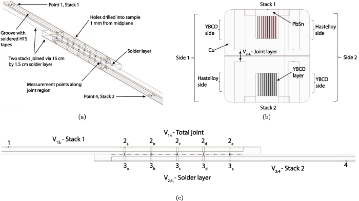
Figure 5. Different views of two overlapping soldered HTS stacks: (a) Overview of the two HTS stacks (embedded in stainless steel not shown), (b) Cross section of the overlapping stacks showing the voltage tap holes, (c) Lengthwise view of the voltage tap probes along the length and relevant labels. In (c), the dashed line is the joint connected region which is either solder in the VPI joints, or copper in the ideal joints.
Download figure:
Standard image High-resolution imageThe holes drilled into the sample are 1.57 mm in diameter. Standard electrical wire is stripped and connected to the bottom of the hole with an electrically conductive epoxy. The voltage taps are solder connected to a multi-channel data acquisition system. A power supply is connected to the sample via current leads attached to each of the copper conductors. The sample is placed in a cryostat which is filled with liquid nitrogen (77 K). The supply is ramped at a rate of 10 A/s and the voltage is collected with 0.1  resolution. For this ramp rate and geometric configuration, the inductive component of the voltage is negligible.
4. Computational study of superconducting stack joints
Before presenting the VPI soldered joint results, it is important to gain understanding of the contributions to the joint resistance in the form of the V12, V23, and V34 components, without the possibility of an imperfect solder layer affecting the measurements. To assist with this effort, a finite element computational model is built and tested against a series of experimental ideal joints, an example of which is seen in figure 6; these are defined as a connection between two superconducting tape stacks which are joined by the same piece of copper such that there is no solder joint. Computational modeling in superconducting coils and devices thus far has been limited to circuit models with coarse spatial resolution. In this section, a spatially refined finite element COMSOL model is presented for predicting current transfer and potential profiles between superconducting stacks. The results give joint resistance predictions, allow comparison with the experimental work, and enable extrapolation to joint resistances for fusion reactor scenarios.

Figure 6. An ideal joint between two superconducting tape stacks, whereby the connection is facilitated by the same piece of copper rather than a solder joint.
Download figure:
Standard image High-resolution image4.1. COMSOL modeling
First, a series of less refined bulk models were built, whereby the HTS tapes and solder matrix are merged into one smeared domain. Although the electrical results of these models are computed rapidly, they do not produce satisfactory results to predict current transfer and joint resistances. To build a highly refined model in COMSOL, the stack and joint components are broken down to their most fundamental domains. In this model, individual tapes are broken down into three components; a 10 µm external copper layer, a 30 µm hastelloy substrate, and a 2–10 µm YBCO layer. Figure 7 shows the breakdown of all the tape layers. The silver layer in between the YBCO and the copper is excluded, and the ceramic buffer layer between the YBCO and the hastelloy is modeled as an electrically insulating surface. An interfacial resistivity of  [15] is applied as the contact impedance on the surface between the YBCO and the copper, representative of that between the YBCO and Ag in an actual tape. Various values for this parameter have been reported in the literature, some as high as
  [16], however tape manufacturing has improved and the most recent values [15] are used. To model the tape stack as in the experiment, each HTS tape is set to be 50 µm above the copper; this is consistent with the 50 µm layer of ribbon solder placed at the bottom of the groove during the solder process.

Figure 7. Labeled individual layers of an HTS tape [21]. 'YBCO side' and 'Hastelloy side', as used in this paper, denote the side of the tape to which the corresponding material is closer.
Download figure:
Standard image High-resolution imageThe domain with the smallest finite elements (YBCO) effectively sets the total number of degrees of freedom, as the mesh of neighboring domains must nodally align. To model domains along the length of the joint, the most appropriate method is to first apply a Quadrilateral mesh to the cross sectional face, and then Sweep this face discretely along the length of the domain. This particular meshing sequence is applied to the YBCO, hastelloy, external Cu layer, solder matrix, and Cu conductor, in that order. Figures 8(a) and (b) show the mesh profiles for both an individual tape, and 10 tapes embedded into a solder matrix, respectively. Figure 8(c) shows the partially meshed surrounding copper conductor. When meshing, two main challenges arise; increasing the number of tapes, and decreasing the thickness of the YBCO layer. Both significantly increase the computational expense of the simulation. It was possible to model 10 tapes with 2 µm YBCO layers, which are of realistic thickness, but to model 40 tapes for consistency with most of the experiments, an extrapolation is required due to the intractability of the system computationally. As such, the assumption is made that the volume of HTS in a particular simulation should be kept consistent with what is present in a given experiment; 10 tapes with 8 µm YBCO layers, 20 tapes with 4 µm YBCO layers, 30 tapes with 2.67 µm YBCO layers, and 40 tapes with 2 µm YBCO layers are systems with the same volume of YBCO. By fitting a curve of the total joint resistance from the 10, 20, and 30 tape tractable cases, simulations of 10 tapes with 8 µm YBCO layers can be completed and extrapolated to the case of 40 tapes with 2 µm YBCO layers (equivalent to the demountable joint experiments), to determine the predicted joint resistance.

Figure 8. Labeled mesh profiles at different scales of the model: (a) Single HTS tape embedded into solder matrix, (b) 10 HTS tapes embedded into a solder matrix, (c) partial meshing of the surrounding copper conductor.
Download figure:
Standard image High-resolution imageThe first set of joints simulated are the ideal joints with no solder layer in between the HTS stacks; the connection is a single solid piece of copper the same length and width as the joint solder layer (15 cm by 1.5 cm). This allows for comparison with experimental joints of the same form, whereby the quality of the solder layer cannot influence the measurement of effective resistance to exit one stack and enter the other. These simulations are performed with material properties at 77 K and 0 T;  Sm−1,
Sm−1,  Sm−1,
Sm−1,  Sm−1,
Sm−1,  Sm−1. Figure 9 shows a series of the current density and electric potential profiles from HTS stacks with 10 tapes and 8 µm YBCO layers. The importance of YBCO orientation with respect to the ceramic buffer layer and the hastelloy is observed. In figures 9(a) and (b), the HTS tapes in the upper and lower stacks are in exactly opposite orientations. In each stack, a tape on one end is facing outward to the copper such that there is an effectively unimpeded path for current transfer, while the tape on the other end is facing inward such that the ceramic insulating layer prevents effective use of the copper for current transfer. This is also reflected in the electric potential profile. The end tapes are found to dictate these profiles. In figures 9(c) and (d) the tapes on the ends of both stacks are facing outward, allowing for the most efficient current transfer geometry and minimum resistance. There are some general trends observed in the simulations: (a) Higher volume of YBCO per tape results in lower joint resistances as there is a greater proportion of high conductivity material, and (b) For a given volume of total YBCO, the joint resistance decreases with increasing number of tapes (and simultaneously less YBCO per tape to ensure constant volume); this is because there is greater uniformity of current transfer across the joint region.

Figure 9. The (a) current density and (b) electric potential cross sectional profiles where the tapes in the upper and lower stacks are in opposite orientations. The (c) current density and (d) electric potential profiles where the end tapes in each stack have YBCO closer to the adjacent copper compared to the hastelloy.
Download figure:
Standard image High-resolution image4.2. Comparison with experimental ideal joints
The results of the simulations are compared with two ideal joints built and tested experimentally. One joint has 10 HTS tapes per stack, each separated by a dummy copper tape for more uniform spacing across the groove width, and the other joint has 40 tapes per stack. The joints are assembled as shown in figure 9(a), with asymmetry in the orientation of each tape on the ends of each stack. The 40 tape ideal joint provides a baseline measurement for the VPI soldered joints, which are also fabricated with 40 tapes per stack. Figure 10 presents the I–V traces for the voltage probe measurements on side 1 of the stacks; exiting stack one labeled 'Exit 1: Measured  ', and entering the second stack labeled 'Enter 1: Measured
  '. In this configuration, the voltage to exit stack one is on the side with YBCO closest to the copper compared to the hastelloy. There are up to five sets of data in each plot (
 ), representing the voltage probe measurements for each of the five probe holes in the experiment. Note that there is theoretically asymmetry in these measurements in this given tape configuration, such that the exit stack measurement on one side of the stack, is the same as the enter stack measurement on the second side. The legend and dashed line present the fit of the average voltage traces V12 and V34 to the equation V = IR; from this the effective resistance of this path is determined. Note that the values for these effective resistances are determined from the low current slope of the I–V traces, as piecewise linearity is observed. The low current slope is defined as the first identifiable linear region; this effect will be further touched upon. Finite element modeling of this geometry with 40 HTS tapes has proven intractable thus far, so the next best comparison is an extrapolation based upon a constant YBCO volume assumption and a varying number of tapes, as explained previously. By modeling 10, 20 and 30 tape ideal joints with equivalent total amounts of YBCO in the joint as a 40 tape (2 µm YBCO per tape) system, and then normalizing the fit of the resistances to the 10 tape ideal joint resistance result, the factor ft
is obtained:
), representing the voltage probe measurements for each of the five probe holes in the experiment. Note that there is theoretically asymmetry in these measurements in this given tape configuration, such that the exit stack measurement on one side of the stack, is the same as the enter stack measurement on the second side. The legend and dashed line present the fit of the average voltage traces V12 and V34 to the equation V = IR; from this the effective resistance of this path is determined. Note that the values for these effective resistances are determined from the low current slope of the I–V traces, as piecewise linearity is observed. The low current slope is defined as the first identifiable linear region; this effect will be further touched upon. Finite element modeling of this geometry with 40 HTS tapes has proven intractable thus far, so the next best comparison is an extrapolation based upon a constant YBCO volume assumption and a varying number of tapes, as explained previously. By modeling 10, 20 and 30 tape ideal joints with equivalent total amounts of YBCO in the joint as a 40 tape (2 µm YBCO per tape) system, and then normalizing the fit of the resistances to the 10 tape ideal joint resistance result, the factor ft
is obtained:


Figure 10.
I–V curves for the 40 tape experimental ideal joint with fitted effective resistances: (a) V12 Exit stack side 1, (b) V34 Enter stack side 1. Colors represent measurable voltage taps ((a)  and (b)
  ) along side 1 of the joint.
Download figure:
Standard image High-resolution imageThis factor is used to scale the 10 tape joint resistance to the joint with number of tapes nt
= 40. The computational and experimental results are displayed in table 1. There is a discrepancy of 29 for the Exit 1 (Stack 1, Side 1) resistance and 26
 for Enter 1 (Stack 2, Side 1) resistance; these results reproduce the asymmetry expected in this tape configuration. The calculated total resistance of
  nΩ also shows good agreement with the theoretical extrapolated value of 16.9 nΩ (a 32
 discrepancy). One of the major reasons for the difference between the theoretical and experimental results is likely an imperfect solder bond between the tapes and the copper, due to the poor distribution of solder that can occur when there is a high number of tapes packed into a small groove. An additional effect on solder distribution could be improper fluxing pre-soldering.
Table 1. Listing of the Total, Exit, Enter experimental measurements (Exp) and the COMSOL results for the 40 tape ideal joint and the 10 tape ideal joint. Exit 1 and Exit 2 denote the measurements from side 1 and 2 of stack 1. Enter 1 and Enter 2 denote the measurements from side 1 and side 2 of stack 2. The corresponding discrepancies ( ) are also tabulated as percentages in brackets next to the experimental results. The uncertainties are the standard error in the fit parameter.
| Ideal stack comparison (nΩ) | |||||
|---|---|---|---|---|---|
| V12 | V12 | V34 | V34 | ||
| Total | Exit 1 | Exit 2 | Enter 1 | Enter 2 | |
| 40 Tape COMSOL | 16.9 | 7.3 | 8.8 | 8.8 | 7.3 |
| 40 Tape Exp |
 (32 (32 ) ) |
 (29 (29 ) ) | — |
 (26 (26 ) ) | — |
| 10 Tape COMSOL | 27.0 | 12.0 | 13.9 | 13.9 | 12.0 |
| 10 Tape Exp |
 (2 (2 ) ) |
 (6 (6 ) ) |
 (9 (9 ) ) |
 ( ( ) ) |
 (11 (11 ) ) |
There were three main purposes for building the second 10 tape ideal joint; (a) Reproduce the asymmetry predicted in this HTS stack configuration (test both sides of the stack—not done in the 40 tape ideal joint), (b) Observe piecewise linear behavior and its correlation with number of tapes, and (c) Compare experimental results to an identical number of tapes in COMSOL with exact YBCO thickness of 2 µm. In order to improve uniformity of the tapes across the groove, a single copper dummy tape is inserted in between each HTS tape. In this experiment, both sides of the stack were measured, to check the asymmetry due to tape face orientation. The results are shown in figure 11. Note the 10 tape ideal joint has a significantly lower critical current compared to the 40 tape ideal joint; thus, in addition to the predominantly ohmically resistive portion of the I–V curve, the data could be measured past the superconducting transition, which is seen at approximately 800 A. In figure 11(a), the blue traces are the  traces from side 1 labeled 'Exit 1: Measured
  ', and the green traces are the
  from side 2 labeled 'Exit 2: Measured
  '. In figure 11(b), the blue traces are the
  traces from side 1 labeled 'Enter 1: Measured
  ', and the green traces are the
  from side 2 labeled 'Enter 2: Measured
  '. The measurable I–V traces from probes on each side of either stack are averaged and the low current slope is fit to the ohmic resistance model, as with the 40 tape ideal joint; the corresponding resistance is displayed in the legend. Indeed the asymmetry expectation holds, with average measurements of 12.7 and 15.1 nΩ for either side to exit stack 1, and 13.9 and 10.7 nΩ for either side to enter stack 2. The computational results for the corresponding measurements are 12.0 and 13.9 nΩ for the YBCO and hastelloy sides, respectively. The discrepancies between all four measurements and the computational results are between 1%–11
 , as shown in table 1. The total calculated resistance shows almost exact agreement with the highly representative computational model, with only a 2
 discrepancy. There could be several reasons why the measured resistance of 10.7 nΩ is less than the computed one of 12.0 nΩ for the YBCO side of stack 2: (1) The copper dummy tapes are not included in the COMSOL model and this would lower the resistance, and (2) The low number of tapes means their natural curvature, due to being wound on a reel, has a big effect on their position in the groove. The side to which the tapes curve closer could result in a lower resistance.

Figure 11.
I–V curves for the 10 tape experimental ideal joint with fitted effective resistances: (a) V12 Exit stack side 1 and side 2, (b) V34 Enter stack side 1 and side 2. In (a), the blue and green traces are the  traces from sides 1 and 2, respectively. In (b), the blue and green traces are the
  traces from sides 1 and 2, respectively.
Download figure:
Standard image High-resolution imageWhen comparing the V14 total joint I–V curves for both ideal joints as seen in figure 12, it is found that the piecewise linearity is more apparent in the 10 tape ideal joint than in the 40 tape ideal joint. This is possibly due to the smoothing of the distribution of tape distances from the joint mid-plane, reducing the disparity of resistive paths through the joint region. This also results in a more uniform current density and tape filling distribution, ultimately reducing the increase in effective resistance with increasing current.

Figure 12. Comparison of the 10 tape and 40 tape V14 total joint I–V curves. The black dashed and dotted lines represent the geometric resistances. The red, yellow and blue dashed lines represent distinct increases in the effective resistance for the 10 tape ideal joint.
Download figure:
Standard image High-resolution imageThe results from the 40 tape ideal joint and the 10 tape ideal joint validate the COMSOL model, and indicate that this finite element framework could be applied to different joint geometries to predict resistivities. The importance of tape orientation is established. The I–V traces show piecewise linearity in the pre-superconducting transition region; from the low current slope, the effective resistances are extracted. This will be denoted as the geometric resistance Rg , a thorough explanation of which is to come in section 4.3. This geometric resistance does not include the resistance due to REBCO transitions at higher currents, and is thus the reference measurement for these experiments. Finally, baseline results for the effective resistances to exit and enter an HTS stack on the YBCO and hastelloy tape sides have been determined, without the influence of an imperfect solder layer. These results will be important when taking into account thermal cycling of the VPI solder joints, and extrapolating the experimental measurements to lower temperatures.
4.3. Modeling the R(I) non-linear dependence
One of the notable observations in the I–V traces for the experimental ideal joints was the piece-wise linearity seen with increasing input current. Particularly in the low  operating regime, it might be expected that the traces are free of superconducting transitional behavior. But a joint consists of individual tapes, each likely at a different distance from the joint midplane, meaning that the current is not uniformly carried in each tape. For current to seek the path of lowest resistance, it must initially find the tape which is closest to a corresponding tape in the other stack. As the current increases, the Ic
of this tape is approached and current shifts to the next lowest resistance tape pair, and so on and so forth. To model the voltage profile, each transition seen can be modeled as a 0D two tape system as represented by the circuit in figure 13; parallel current pathways, each with a variable resistor RSC
representing the HTS tape, and with a standard resistor R symbolizing the solder and copper distance under each tape (distance to the corresponding tape). This model is treated as a quasi-steady process and thus the self and mutual inductances are ignored. In addition, to reduce model complexity to that needed to investigate the behavior of interest, the solder contact layer in between the two tapes is ignored. Using Kirchhoff's voltage law for this system, the following equation is obtained:
operating regime, it might be expected that the traces are free of superconducting transitional behavior. But a joint consists of individual tapes, each likely at a different distance from the joint midplane, meaning that the current is not uniformly carried in each tape. For current to seek the path of lowest resistance, it must initially find the tape which is closest to a corresponding tape in the other stack. As the current increases, the Ic
of this tape is approached and current shifts to the next lowest resistance tape pair, and so on and so forth. To model the voltage profile, each transition seen can be modeled as a 0D two tape system as represented by the circuit in figure 13; parallel current pathways, each with a variable resistor RSC
representing the HTS tape, and with a standard resistor R symbolizing the solder and copper distance under each tape (distance to the corresponding tape). This model is treated as a quasi-steady process and thus the self and mutual inductances are ignored. In addition, to reduce model complexity to that needed to investigate the behavior of interest, the solder contact layer in between the two tapes is ignored. Using Kirchhoff's voltage law for this system, the following equation is obtained:


Figure 13. 0D circuit model used to predict the piece-wise linearity observed in the voltage profile.
Download figure:
Standard image High-resolution imagewhere the subscripts 1 and 2 denote each current pathway. Furthermore the values of  A, n = 20,
  V,
V,  nΩ and
  nΩ, and the equation
  are used. The system can then be solved for I1 and I2 with a sweep of the input current Itot, using the Matlab in built function 'vpasolve'. The different resistances for each pathway imitate the varying distance of a given tape from the corresponding tape in the other stack. Figure 14(a) shows the individual current in each tape with increasing total current. As expected, most of the current is contained in tape 1 until the critical current is reached. At this point more current starts to fill tape 2, until both tapes carry equal current when they become non-superconducting. In figure 14(b), the voltage profiles of various components are seen. The 'Stack Voltage' is defined as
  , and shows the piecewise linearity in the I–V trace as seen in the experiments (figures 10–12). The effective resistance in this model can be defined as
  ; when this is plotted (figure 14(c)), the first slope is a constant, and the second, a rising resistance with increasing current. The constant resistance corresponds to the geometrical resistance Rg
based purely upon the materials and the geometry of the system, and in this example is equal to 4 nΩ; a simple calculation of two parallel paths gives this result
; when this is plotted (figure 14(c)), the first slope is a constant, and the second, a rising resistance with increasing current. The constant resistance corresponds to the geometrical resistance Rg
based purely upon the materials and the geometry of the system, and in this example is equal to 4 nΩ; a simple calculation of two parallel paths gives this result  . Between
  A to
A to  A the effective resistance increases with current, indicating that the contribution is not purely geometrically based; while a higher share of the current is now carried by the pathway through tape 2, there is a contribution from the continually increasing superconducting transitional resistance of tape 1. As seen in figure 12, this observation of piecewise linearity is more present in the experiments that contain less tapes, where as it is more subtle in those with a higher number of tapes; this is possibly due to the smoothing of distribution of tape heights from the joint mid-plane, resulting in less discrepancy between resistive paths through the joint.

Figure 14. Circuit modeling results showing (a) individual tape currents, (b) voltage components present in the stack (c) effective resistance of the joint.
Download figure:
Standard image High-resolution imageThis simple model reproduces the piecewise linearity observed in the experimental results, and supports the hypothesis that tapes are filled with current in an order dependant on their distance from the joint midplane. Following the presentation of the electrical results from the VPI soldered joints, the applicability of the low current I–V slope effective resistance measurement in the case of high current conditions, will be addressed.
5. Experimental campaign: electrical results
5.1. 77 K electrical measurements
The electrical testing results at 77 K for the VPI low temperature solder demountable joints are presented in this section. Seven VPI solder joints were built; the differences and iterations between each joint and the correlation with electrical performance are discussed. In table 2, the values listed represent the geometric resistance as determined by the low current I–V slope, in accordance with interpretation from the computational model.
Table 2. The effective resistance (nΩ) is documented for all the joints built with 40 tape stacks. In the joint description, the thickness of the joint (µm), the type of solder used, and the flux used (RMA or TAC-012) is documented. 'Polish' denotes the extra fine polish steps taken for the steel and copper; this was done for all joints beyond joint 2. 'NSC' denotes 'no side channel', so that solder flows through the joint groove rather than through the side channel; this was done for all joints beyond joint 3. Shown are the effective resistances as calculated from the average voltages for Exit stack (V12 Exit 1 - Side 1/YBCO Side, and V12 Exit 2 - Side 2/Hastelloy Side), the average voltages for Enter stack (V34 Enter 1 - Side 1/Hastelloy Side, and V34 Enter 2 - Side 2/YBCO Side), and the average voltages for Solder layer (V23 Side 1, and V23 Side 2). This was only done completely for joints 8 and 9. Total (V14) denotes the overall joint resistance, as measured between probes 1 and 4.
| Effective Resistance (nΩ) | |||||||
|---|---|---|---|---|---|---|---|
| V12 | V12 | V34 | V34 | V23 | V23 | ||
| Total | Exit 1 | Exit 2 | Enter 1 | Enter 2 | Solder 1 | Solder 2 | |
COMSOL: 75µm 
| 20.3 | 7.13 | 8.67 | 8.67 | 7.13 | 4.71 | 4.71 |
Joint 1:  m m  , RMA , RMA | 39.7 | — | — | — | — | — | — |
Joint 3:  m m  , RMA, NSC , RMA, NSC | 32.5 | 8.7 | — | 13.4 | — | 8.6 | — |
Joint 4:  m m  , RMA, No VPI , RMA, No VPI | 36.2 | 9.9 | — | 12.2 | — | 14.1 | — |
COMSOL: 137.5µm 
| 23.5 | 7.13 | 8.67 | 8.67 | 7.13 | 7.92 | 7.92 |
Joint 2:  m m  , RMA, Polish , RMA, Polish | 38.9 | 12.9 | — | 14.7 | — | 9.9 | — |
Joint 7:  m m  , TAC 012 , TAC 012 | 36.1 | 12.5 | — | 14.0 | — | 9.8 | — |
Joint 9:  m m  , TAC 012 V2 , TAC 012 V2 | 35.4 | 7.2 | 12.2 | 16.5 | 15.5 | 8.7 | 9.7 |
COMSOL: 137.5 µm 
| 17.6 | 7.13 | 8.67 | 8.67 | 7.13 | 1.96 | 1.96 |
Joint 5:  m m  Pressure Pressure | 29.4 | 9.7 | — | 14.7 | — | 3.9 | — |
Joint 6:  m m  , RMA , RMA | 33.2 | 9.5 | — | 17.8 | — | 3.6 | — |
Joint 8:  m m  , TAC 012 , TAC 012 | 32.9 | 10.0 | 11.8 | 19.4 | 18.4 | 2.8 | 3.1 |
COMSOL: 137.5 µm 
| 21.3 | 7.13 | 8.67 | 8.67 | 7.13 | 5.68 | |
Joint 10:  m m  , 1 M HCl , 1 M HCl | 33.9 | 8.1 | — | 14.9 | — | 9.3 | — |
5.1.1. Documenting joint measurements and characteristic labels
Results for ten assembled joints are listed, seven of which are the VPI demountable joints. An example of a VPI demountable joint with all voltage probes attached is seen in figure 15. For the other three joints, joint 4 was a soldered joint assembled without a VPI process, joint 5 was an indium compression (pressure) joint, and in joint 10 the gallium was flowed in an identical setup to the VPI system but at atmospheric pressure. It is also noted that the HTS tape orientation is in the same configuration as in the ideal joints. The calculations are split up into the YBCO side and hastelloy side for stack 1 (current exits stack 1) and stack 2 (current enters stack 2). From figure 5(b), one can see the left side of the stacks is denoted as side 1, and the right side of the stacks as side 2. In the table the results from side 1 are listed as 'Exit 1' (YBCO side), 'Enter 1' (hastelloy side), 'Solder 1', and the results from side 2 are listed as 'Exit 2' (hastelloy side), 'Enter 2' (YBCO side), and 'Solder 2'. Only two joints (joints 8 and 9) were probed on both sides. The joints are labeled in the chronological order (joints 1–10) in which they were built, so that updates between joints can be explained in the context of the results seen in a previous joint. 'Total' is the total joint resistance as determined from the V14 voltage measurement. The other way to determine the total joint resistance is to add the effective resistances as determined from the V12, V23 and V34 measurements.

Figure 15. Set of probes attached to the single channel VPI demountable joint. To the left and right are seen voltage taps V1 and V4, respectively. In the joint region, there are voltage taps on both sides of the stack which are color coded and match the corresponding point on the opposite stack side.
Download figure:
Standard image High-resolution imageNote that the addition of these three resistances is between −2.3 and 0.2
  different from the V14 measurement across the joints, or on average 0.9
  smaller. For most of the joints the discrepancy is on the smaller end of this scale, possibly caused by fluctuations in the voltage measurements. For the larger discrepancies, this is more likely indicative of the quality of the voltage tap connections. The average negative bias difference of the three sub measurements compared to the V14 measurement, could be due to the difference in the soldered voltage taps (points 1 and 4) and the electrically conductive epoxy voltage contacts (points 2 and 3), in which case the majority of the discrepancy would be split across the effective resistances to exit and enter the HTS stacks. While the small differences should be noted, they are not crucial to the work going forward. The analyses of the three effective resistances will be conducted via the V12, V23, V34 measurements; aside from the standard uncertainty from the variation amongst voltage probes for a given effective resistance, a second uncertainty could be added based upon an equal division of the discrepancy magnitude between total resistance calculation methodologies.
To label a joint in the table, the machined joint thickness, type of solder, and type of flux (RMA or TAC-012 or HCl) are listed. The 'No VPI' label was specific only to joint 4; this joint was assembled without a VPI process. The 'Pressure' label denotes that joint 5 was an indium compression joint. The 'Polish' and 'No side channel' (NSC) labels are changes that applied to all VPI joints going forward; all copper joint surfaces were polished to eliminate most machining scratches from joint 2 onward, and solder was forced directly through the joint layer (designed solder flow side channel blocked off) for all joints from joint 3 onward. Figures 16 and 17 show the sample average I–V traces for the V12 Exit, V34 Enter, and V23 Solder layer voltage measurements, respectively; these are from side 1 or the left side of the stacks, with the fit values listed for the corresponding effective resistances. The equivalent I–V traces from the computational model and the associated resistances are listed for comparison. In many of the V12 and V34 I–V curves, there is piecewise linearity present in the current range tested.

Figure 16. I–V curves for all joints showing (a) Exit V12 side 1 (b) Enter V34 side 1. Also plotted are the COMSOL modeling results.
Download figure:
Standard image High-resolution image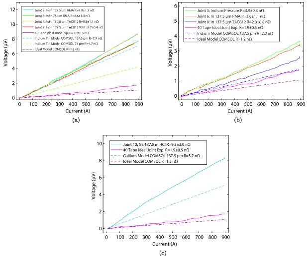
Figure 17. I–V curves for all the V23 side 1 solder layer measurements showing the results from (a) InSn solder joints, (b) In solder joints, and (c) the Ga solder joint. Also plotted are the COMSOL modeling results.
Download figure:
Standard image High-resolution image5.1.2. Joint voltage comparisons and the impact of thermal cycling on HTS stacks
The resistances determined from COMSOL from the extrapolated 40 tape case are documented in table 2. To infer the solder layer quality, the V23
Solder measurements in the table are considered; comparison with the computational results from COMSOL shows variable agreement. For 137.5 µm, the lowest discrepancy for the  solder layer was 51
 (1.96 vs. 2.95 nΩ), and for
  , it was 16
 (7.9 vs. 9.2 nΩ); 2.95 nΩ is the average of Solder 1 and Solder 2 in joint 8, and 9.2 nΩ is the average of Solder 1 and Solder 2 in joint 9. For the Exit 1 measurement, the discrepancy varied from nearly exact agreement to as high as 80
 . For the Enter 1 measurement, the lowest discrepancy was 38
 from the theoretical value. The exit and enter stack measurements, while similar in trend and magnitude, vary due to the initial soldering process, and modification from thermal cycling during the VPI processes. This can introduce additional resistance to the measurement for current exiting or entering an HTS stack, as the tapes and surrounding structure can be thermally degraded. The large range of variation in the exit/enter stack resistances, yet good model-experiment agreement for the solder layer, support the hypothesis that there are external (possibly thermal effects) causing damage and variation in the exit/enter stack current pathways. For example, joint 5 and joint 10 use the same baseplate and HTS stack conductors; there was very little heating applied to this joint (indium pressure joint and gallium joint, respectively), resulting in limited variation in the Exit 1 and Enter 1 measurements. Joints 3, 6 and 8 use the same baseplate, showing increases in the Exit 1 and Enter 1 measurements after significant heat application from the cycling to make these joints; joint 3 had a resistance of 32.5 nΩ with an 8.6 nΩ Solder 1 measurement, but the overall resistances of joints 6 and 8 were higher than joint 3 despite a drop in the Solder 1 measurement by ∼5 nΩ. Joint 4 which was very rapidly thermally cycled once during assembly, showed similar Exit 1 and Enter 1 measurements (9.9 and 12.2 nΩ) to the 40 tape ideal joint (9.4 and 11.1 nΩ). For joints 2, 7 and 9, the same baseplates were used; here the overall resistances changed according to the improvement in the solder layer and there was little overall change in the Exit 1 and Enter 1 measurements, however the values (∼12.5 and 15 nΩ) were higher than for the other baseplates, indicating more YBCO damage in the initial soldering process. Note that a separate experimental campaign conducted on the thermal cycling damage on soldered HTS stacks at VPI relevant temperatures will be presented in a future paper. As shown here, there are also situations where there is no significant damage due to this thermal cycling, and this is promising data has also been observed in thermal cycling campaign. It is critical for the viability of the VPI process to facilitate demountable solder joints, that the damage is understood and minimized.
5.2. Iterations during the VPI processes
In this section, the iterations between joints are documented, and the solder joint quality is discussed. Most of the joints were sheared apart by applying tensile load on the INSTRON machine, so that the solder profile was exposed; these results are documented in figure 18. The notable takeaways from the iterations and the resulting data are the following:
- There are very similar total resistance results (as calculated from V14) between the first and second joints with
 , using RMA flux, but with different joint thicknesses of 75 µm (joint 1) and 137.5 µm (joint 2), respectively. During the post mortem analysis of a sheared joint 1, it was seen that the machining finish of the end mill left some grooves in the copper in the joint region (figure 18(a)), resulting in trapped flux bubbles in the groove recesses (figure 18(b)). In addition, there was a large elongated unbonded section (figure 18(c)). To rectify this, a more precise machining process was operated to smooth out the copper surface, and then it was subsequently grinded with increasingly finer grit sandpaper to create a finish with an average surface roughness of less than 1.5 µm. The shearing of the thicker joint 2 showed a significantly improved solder bond at the microstructural level (figure 18(d)). Thus a similar total joint resistance resulted (3 improved); 39.7 nΩ for joint 1 vs. 38.9 nΩ for joint 2, despite the 80 thicker solder layer. While the three voltage components were not measured for joint 1, the joint 1 and joint 3 baseplates and HTS conductors are the same; thus under the assumption that the Exit 1 and Enter 1 measurements for joint 1 are equivalent or less than those for joint 3, the solder layer dominates the change in the joint resistance between joints 1 and 2. This indicates the importance of a highly smoothed surface finish to the soldering quality. Note that while the microstructural bonding improved significantly, there still existed a large elongated unbonded section in joint 2.
 - Between joints 2 and 3, aside from the reduction in the joint thickness from 137.5 µm to 75 µm, the main change was to block the side channel designed for solder flow with a square silicone rubber gasket (NSC = No Side Channel). The purpose of this was to force the solder through the joint groove, with the goal of improving the overall area soldered; in the previous two joints, there was a very similar overall soldering profile (figures 18(c) and (d)) with an elongated unbonded section, possibly indicative of how solder inefficiently wicks from the side channel to the solder layer. Forcing the solder directly through the solder joint layer resulted in a significantly improved overall solder profile (figure 18(e)) without a large unbonded section. Thus for joints with the same solder layer thickness of 75 µm, this resulted in an 18 reduction in the total joint resistance (from V14); 39.7 nΩ for joint 1 vs. 32.5 nΩ for joint 3.
- Changing from RMA flux to TAC-012 flux resulted in improvements in the overall joint resistance. TAC-012 is a more pasty/viscous flux, which becomes liquefied with the application of heat, and is specific for indium based solders and oxides. This indicates the importance of flux selection for the quality of the solder process. For , the solder layer resistance improved 18 between joint 6 (RMA) and joint 8 (TAC-012); note one can see that the bonding quality is already quite high in joint 6 (figure 18(g)). A small total improvement of 7 is also seen between joints 2, 7 (figure 18(h)) and 9 for the layer measurement. Note that for joints 8 and 9, the average of both Solder 1 and Solder 2 can be used, as unlike the other measurements, these should theoretically be identical.
- The 'No VPI' joint (joint 4) was comprised of two superconducting stacks with a 75 µm solder gap, clamped and soldered by hand. The purpose of this joint was to enable comparison of a rapidly assembled joint in atmospheric pressure conditions. The Solder 1 measurement indicates that the bonding quality of this joint was not comparable to the quality attained in the VPI process.
- The indium pressure joint (joint 5) was used to compare the difference between the highest performing compression joint and the solder joints. The performance across the joint layer (V23) was within of the highest performing indium solder joint (joint 8), indicating that the contact resistance () between the indium wire and the copper surface is so low as to make a compression joint (figure 18(f)) perform almost as well as the pure indium solder joint. Note the measured thickness of the compressed indium was approximately 125–150 µm, in the range comparable to the solder joints. This is not a surprising result due to the malleability of indium causing it to conform around the copper surface asperities; however, the pure indium solder joint has slightly better performance, likely due to the good intermetallic bond between the solder and the copper. The higher exit and enter stack resistances present on the pure indium solder joints are likely due to the temperature exposure associated with the VPI process, resulting in thermal degradation of the HTS stacks.
- The re-soldering of an (V2) joint with TAC-012 (joint 9) was specifically to measure the voltages on both sides of the stack, which was not done in the earlier joints. The previous joint (figure 18(h)) had also been sheared in the INSTRON to check bond quality, so the chance to repeat the VPI process with the same solder and flux opened the opportunity to test joint result repeatability. A more dense layer of TAC-012 flux was used in this process; the average of the Solder 1 and Solder 2 measurements of 9.2 nΩ improved upon the joint 7 value. This result gives high confidence of the repeatability of the VPI process and subsequent joint performance.
- The final joint built (joint 10) was with gallium (99.9999). Gallium's low melting point of 29.8 C and its good electrical conductivity make it a joint solder candidate with promise; in particular, the low process operating temperature means HTS stack thermal degradation would be minimized compared to the other solders. An identical setup without vacuum was used to flow the gallium. The reason for flowing the at atmospheric pressure is that the vacuum would cause evaporation and crystallization of the HCl required to remove oxides. HCl effectively acts as the flux for the wetting and reaction between copper and gallium. A 1 M solution of HCl requires only ∼38 C for activation, thus the oven temperature was set to 50 C for this process. The joint had a larger error between the experimental and theoretical predictions than did all of the other joints. The result across the joint layer of nΩ was comparable to the best result across the joint layer of nΩ (average of V23 measurements in joint 9). This is despite the difference in resistivity of gallium ( Sm−1) and solder ( Sm−1). The gallium joint was separated (with very little force) in order to investigate the microstructure. The entire joint surface was well coated in gallium (figure 18(i)), although there was a very weak bond between the gallium bulk and the intermetallics on the copper surface. While there are challenges in working with gallium, the combination of low process operating temperature to minimize HTS stack degradation, and high electrical conductivity at cryogenic conditions, make it worth pursuing in further experiments. One may also consider gallium alloys which contain indium and/or tin for improved wettability and structural integrity.


Figure 18. The joints that were sheared apart on the INSTRON machine are documented: (a) Joint 1: close up showing the milling scratches and resulting unbonded regions. (b) Joint 1: development of voids in the solder due to flux bubbles. (c) Joint 1: unbonded elongated section seen, likely due to solder flow channel. (d) Joint 2: improved quality of the bonding microstructure as compared to joint 1, but still an unbonded elongated section. (e) Joint 3: uniform bonding profile resulting from forcing solder flow directly through groove. (f) Joint 5: indium wire compression joint. (g) Joint 6: indium solder joint showing high uniformity and bonding fraction (h) Joint 7: indium tin solder joint with high bonding fraction. (i) Joint 10: gallium solder joint showing the structure of gallium at micro thicknesses.
Download figure:
Standard image High-resolution image5.3. Extrapolating 77 K results to 10 K
Consideration of the Solder layer allows for optimization of the VPI process and understanding of the solder quality. Ultimately however, the total joint resistance is the relevant quantity when aiming to satisfy the joint requirements laid out previously. In addition, it is of interest to find a scaling methodology to extrapolate the 77 K electrical measurements to fusion magnet relevant temperatures  K. In order to present a resistance value which encapsulates the entire joint (exit stack, solder layer, enter stack) and allows for comparison across joints, the variation amongst the exit and enter stack values must be taken into account. As the joints were heated, cycled and reused, the resistances to enter and exit the stack in some cases increased on average. There is also uncertainty and variance in the manufacturing of the HTS stacks in the solder quality, tape density, and tape distance from joint midplane. All of this variation manifests in the current pathways into and out (exit, enter) of a stack. At 77 K, the solder layer contributes a minor portion to the overall joint resistance, so these exit and enter stack measurements can mask the differences in joint performance based upon the quality of this solder layer. One method of comparison of the total joint resistance that takes into account this variation, is to use the effective resistance values to exit and enter the stacks calculated from the 40 tape ideal joint experiment;
  nΩ and
  nΩ.
nΩ.
Table 3 presents the total joint resistivities in various formats. In column one labeled 'Normalized', the resistivity presented is the normalized total resistivity calculated from the equation:

Table 3. Column 1: 77 K Normalized resistances, Column 2: 77 K Measured resistances, Column 3: 10 K Extrapolated normalized resistances, Column 4: 10 K Extrapolated measured resistances. This table compares the normalized and measured resistance values at 77 K. In addition, the extrapolated values of the performance of these joints based upon COMSOL electrical resistivity ratios are determined for a temperature of 10 K. The area used in these calculations Aj is 15 cm by 1.5 cm.
Normalized and Measured Total Joint Resistivities Rj
( ) ) | ||||
|---|---|---|---|---|
| R 77 K Normalized | R 77 K Measured |
 10 K Extrapolated from R 77 K Normalized 10 K Extrapolated from R 77 K Normalized |
 10 K Extrapolated from R 77 K Measured 10 K Extrapolated from R 77 K Measured | |
COMSOL: 75 µm 
| 0.460 | 0.460 | 0.111 | 0.111 |
Joint 1:  m m  , RMA , RMA | — | 0.893 | — | — |
Joint 3:  m m  , RMA, NSC , RMA, NSC | 0.655 | 0.691 | 0.182 | 0.187 |
Joint 4:  m m  , RMA, No VPI , RMA, No VPI | 0.779 | 0.815 | 0.254 | 0.260 |
COMSOL: 137.5 µm 
| 0.532 | 0.532 | 0.159 | 0.159 |
Joint 2:  m m  , RMA, Polish , RMA, Polish | 0.684 | 0.844 | 0.200 | 0.224 |
Joint 7:  m m  , TAC-012 , TAC-012 | 0.682 | 0.817 | 0.198 | 0.219 |
Joint 9:  m m  , TAC-012 , TAC-012 | 0.668 | 0.785 | 0.191 | 0.209 |
COMSOL: 137.5 µm 
| 0.401 | 0.401 | 0.059 | 0.059 |
Joint 5:  m m  Pressure Pressure | 0.549 | 0.637 | 0.078 | 0.089 |
Joint 6:  m m  , RMA , RMA | 0.542 | 0.695 | 0.077 | 0.099 |
Joint 8:  m m  , TAC-012 , TAC-012 | 0.528 | 0.737 | 0.075 | 0.107 |
COMSOL: 137.5 µm 
| 0.483 | 0.483 | 0.057 | 0.057 |
Joint 10:  m m  , 1 M HCl , 1 M HCl | 0.671 | 0.727 | 0.071 | 0.079 |
where Aj is the area of the solder groove, and Rs is the solder layer resistance as calculated from V23 for each of the joints. This normalized resistivity is what the joint resistivity would be if the variation in the soldered stacks could be mitigated. In column two labeled as 'Measured', the unadjusted original total joint resistivities as calculated from the addition of V12, V23 and V34 are presented. To calculate how impactful these differences are at lower temperatures relevant to a fusion magnet, the equivalent COMSOL system is modeled with electrical properties at 10 K. By taking the ratio of the 10 K and 77 K equivalent voltage differences in the COMSOL model, these factors can then by applied to the experimental data; the extrapolated values are reported in columns three and four. The equation used to calculate the extrapolated resistivities at 10 K can be written as follows:

where  are the sample average measured voltages, and
  are the COMSOL voltages at a temperature of Tj
; both are for a current I. The rows labeled with 'COMSOL' list the values computed directly from the 77 K and 10 K models. Table 3 shows that because of the major drop in the exit and enter stack resistances from 77 K to 10 K, there is a much smaller difference between the measured and normalized values in the 10 K extrapolated joint resistance. At 77 K, it is found that for
are the COMSOL voltages at a temperature of Tj
; both are for a current I. The rows labeled with 'COMSOL' list the values computed directly from the 77 K and 10 K models. Table 3 shows that because of the major drop in the exit and enter stack resistances from 77 K to 10 K, there is a much smaller difference between the measured and normalized values in the 10 K extrapolated joint resistance. At 77 K, it is found that for  , the best measured resistance from the joints built with a solder joint thickness of 137.5 µm is
  with a discrepancy from the COMSOL model of 47
 , where as the normalized resistance of
  has a discrepancy of 26
 . For the pure
  joint with a solder joint thickness of 137.5 µm, the best measured resistance was
  with a discrepancy from COMSOL of 84
 , where as the normalized resistance of
  has a discrepancy of 32
 . For the pure
  joint with a solder joint thickness of 137.5 µm, the best measured resistance was
  with a discrepancy from COMSOL of 51
 , where as the normalized resistance of
  has a discrepancy of 39
 . At 10 K, the discrepancies of the normalized values compared to the COMSOL values for the highest performing joints are between 20%–28
 . To recap, these values are for a 4 mm wide stack, presiding over a 15 cm by 1.5 cm wide solder joint layer. This corresponds to an aspect ratio of
  , where ws
is the stack width and wj
is the joint width; the aspect ratio in a fusion magnet is expected to be 1, based upon the geometry. This implies that the joint resistances achievable will be lower than what is presented here, however these once again validate the model, and its application to predicting fusion magnet joint resistances.
, where ws
is the stack width and wj
is the joint width; the aspect ratio in a fusion magnet is expected to be 1, based upon the geometry. This implies that the joint resistances achievable will be lower than what is presented here, however these once again validate the model, and its application to predicting fusion magnet joint resistances.
Based upon the normalized values, these results also show that at 77 K, the solder layer in fact is only  (
( ) to
) to  (
( ) of the entire joint resistance, the remainder coming from the resistance to exit and enter an HTS tape stack. As shown in the extrapolated 10 K results here, this is greatly modified by the change to lower temperatures relevant to fusion magnets. For example,
  becomes the dominate component of the joint resistance at
  , as the copper and
  solder drop in resistivity more dramatically, where as
  contributes less than 1
 at these temperatures. This is seen in columns three and four in table 3 where the extrapolated normalized values at 10 K are listed; for the
  results, the value listed is almost equivalent to just the exit/enter stack resistances alone. More work needs to be done to both prevent degradation and variation in the current pathways to exit and enter a tape stack, and to prevent piecewise linearity from contributing significantly to the joint resistance. This extrapolation methodology provides a tool which quite accurately predicts the joint resistances at different temperatures, based upon the voltage measurements done at 77 K.
5.4. Resistivity predictions in realistic joint geometries and conditions
Further validation of the model allows for its use in predicting joint resistances at fusion magnet relevant conditions and geometries. A system with aspect ratio of  is considered. The total joint resistance can be written as (
 ):
):

The first term effectively denotes the ideal joint contribution, and the second term effectively denotes the solder layer contribution.  is the tape factor from equation (3), used to simulate the system with 10 tapes and extrapolate to the appropriate tape density used in a fusion magnet (
 tapes/cm; representative of the value used in the large scale non-insulated coil experiments). Δ1 and Δ2 are the smallest fractional discrepancies associated with either term from the experimental measurements. The coefficients
  and
and  are determined for a given set of conditions, materials and geometries; this is completed using electrical resistivity and magnetoresistivity data from the literature. δj
is the solder layer thickness. To present an example, the operating temperature is chosen to be 10 K. Because toroidal field coil joints would likely be in a lower field area, a value of 2 T is chosen. These give
are determined for a given set of conditions, materials and geometries; this is completed using electrical resistivity and magnetoresistivity data from the literature. δj
is the solder layer thickness. To present an example, the operating temperature is chosen to be 10 K. Because toroidal field coil joints would likely be in a lower field area, a value of 2 T is chosen. These give  , and
, and  for
for  ,
,  , and
, and  respectively [5]. The fractional discrepancies are
  (table 1), and
  for
for  ,
,  , and
, and  respectively (table 2). A joint thickness of
  m is chosen to balance the tradeoffs between lower resistance (thinner joints) and longer joint lifetime (thicker joints). Note the lifetime is set by the growth of the solid phase intermetallic layer, a result of the liquid solder/solid substrate bonding; assuming one hour mount and demount cycles for the fusion magnet and 1–2 years between vacuum vessel replacements, 100 µm is a good reference estimate for solder joint operation over the entire reactor lifetime, however joint servicing would be expected at various demounting windows [5]. The values given result in joint resistivities of 38, 125, and 103
  for
for  ,
,  , and
, and  respectively. These results are competitive with the lowest resistance joints presented in the literature for cable geometries.
It is also important to address the question of applicability of these results to high current conditions; as demonstrated in this paper, the joint resistance does not remain constant as the current increases. There are steps that could be taken to reduce the piecewise linearity present in the pre-superconducting transition region, so that the resistance in the low current region is the same as that in the high current region. These include increasing the number of tapes in the stack, and developing a technique to reduce the variation in tape distance from the joint midplane. However without these developments, it is important to gain some quantitative measure of the joint resistances at higher currents. The  ratio is the effective resistance of the joint; this is plotted in figure 19 for three joints that most clearly show the divide between the region defined by the approximately constant geometric resistance, and that of increasing effective resistance. However what is particularly noteworthy is that this effective resistance asymptotes; possibly due to current uniformity and re-distribution within the stack, this suggests that there is not continual and significant increase of the joint resistance at higher currents.

Figure 19. Plot showing the effective resistance  of three joints that most clearly show the divide between the geometric resistance region and that of asymptotically increasing effective resistance.
Download figure:
Standard image High-resolution imageTo infer this effect from a different experiment, the joint resistance can be analyzed from the recent SPARC TFMC, built and tested to high current and high field at the PSFC. A series of papers have been published on the experimental and modeling results from the TFMC campaign [22, 23]. This coil was operated at 20 K and had indium compression joints between no-insulation pancakes. For local fields at the joints of 0, 6, and 14 T (operating current ∼1, 40, 40 kA respectively), the joint resistances are 0.5, 1.2, and 1.6 nΩ, respectively. When adjusting for the TFMC stack width and copper thickness in the model, and computing results at the relevant field and temperature conditions, the joint resistances predicted are 0.44, 1.08, and 1.26 nΩ, respectively. It is noted that the aspect ratio of the TFMC joints is not captured in this exercise, but given the large width of the HTS stack and the lack of copper directly to the side of the HTS tapes which would allow for more efficient current transfer, modeling this is expected to reduce the predicted joint resistances by only a small fraction. At the highest field case, there is a 27 discrepancy between the TFMC measured joint resistance and the model. This comparison gives good confidence that the increase in the total effective joint resistance from the low current slope is only marginal. To summarize the results of this exercise, it is seen that the increase of the effective total joint resistance due to higher current non-linearity is not significant. The small increase is likely due to a combination of a high number density of tapes which smooth out the distribution of tape heights from the joint midplane, and the fact that there is high tension on these tapes in the TFMC pancakes during the winding process and in soldering, reducing the variation in tape heights from the joint midplane. At a minimum, these same conditions should be present in a fusion magnet, demonstrating the applicability of these results to high current conditions. It should also be noted that good agreement between the TFMC measured joint resistivities and the model predictions, in addition to good agreement between the 10 K VPI joint extrapolated results (from 77 K) in table 3 and the model, demonstrates the reliability of the temperature extrapolation methodology. While 77 K measurements of the TFMC were not completed, more temperature comparisons would be useful to further calibrate this approach, in the case that only 77 K (or higher than operating temperature) measurements are possible at an early stage of a testing campaign.
5.5. Demounting: reversing the process
There was no part of this experimental campaign dedicated to cycling or re-soldering the joints; they were cleaned each time a new solder or design change was tested in the VPI process. However, the first step in the re-use of a joint was implemented; the demountability of the joint by reversing the VPI process. Vacuum is drawn on the solder channel, and the joint is reheated to the operating temperature required to mount it, melting the low temperature solder. Pressurized argon is flowed to push the solder directly out of the joint regions, and into a solder dump. This test was conducted with both an  joint, and an
  joint. While still hot, the samples were unbolted and disconnected with ease. Figures 20 and 21 show the results of both of these tests. In summary, both were successful; solder was pushed into the solder dump, and the joint surfaces had no significant excess solder.

Figure 20.
 joint demounted using the reverse argon VPI process. (a) A close up of the surface showing various areas which are not bonded. These nonbonded areas are heavily oxidized and fouled with crystallized flux. (b) Zoomed out image of the entire joint region post blow out.
Download figure:
Standard image High-resolution image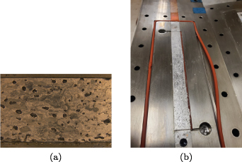
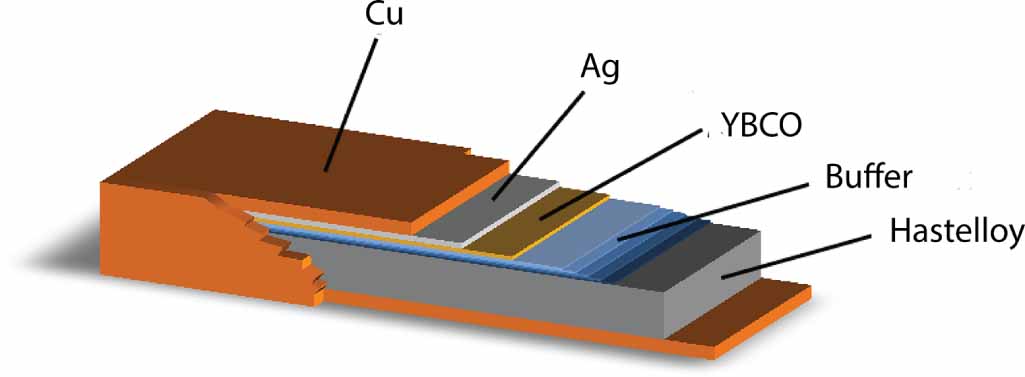
Figure 21.
 joint demounted using the reverse argon VPI process. (a) A close up of the surface showing that the entire region is very well bonded. Interestingly, there are miniature mounds of indium which appear on the surface and were not cleared out during the blow out. (b) Zoomed out image of the entire joint region post blow out.
Download figure:
Standard image High-resolution image
The  joint tested was one which used RMA flux and the side solder flow channel, producing a more non-uniform bonding profile than when TAC-012 flux was used. This reinforces the importance of using an appropriate flux and having an optimized solder flow path (forcing solder to flow directly through the joint region). Because the unbonded sections in this joint are fouled with crystallized flux, this means that in a remounting process only the already soldered section would be re-soldered, illustrating the importance of performing the first process correctly. It is possible pre-wetting could be considered for the joint pad surfaces, before the first VPI process is conducted.
The demounted  sample showed much better bonding uniformity. Infact, all of the pure indium joints in general showed improved uniformity over the
  joints, in spite of which flux was used. Once again most of the solder layer was cleared out, however there were small clumps of indium or indium based alloys on the wetted surface. It is possible these were alloys whose melting temperature was higher than that reached in the demounting process, or indium clumps that were simply not molten because there was very little additional temperature margin due to the
  melting point limit.
One of the next phases of testing for the demountable joint program should involve re-soldering a demounted joint and performing the same electrical testing to ensure solder re-wets the substrate surfaces properly, and thus similar joint resistances can be achieved, an essential aspect of the demountable joint. Results in section 5.1 and a comprehensive study to be presented in a future paper show promising data that displays minimal thermal damage on the HTS stack during a VPI cycle, and in addition, the intermetallic phase at the substrate/solder interface is of similar electrical conductivity to the average of the constituting elements; these points support the argument that as long as high quality solder wetting can be achieved in successive cycles, similar joint resistances will be possible. The demounting test proved that the low temperature solder joints are easily demountable by the same process used to mount them: using pressurized argon gas to push molten solder in or out of the joints.
6. Conclusion
Low resistance joints that facilitate demountability are a critical technological component for modular high temperature superconducting devices, including fusion magnets. In this work the superconducting joints of interest were studied computationally via a finite element model, and experimentally via a novel low temperature solder VPI process, to enable demountability and low electrical resistance in a no-insulation coil framework. The joint resistance is analyzed in three parts: the resistance to exit HTS stack one, cross the solder joint layer, and enter HTS stack two. It is determined that the effective resistance for current to exit and enter an HTS superconducting stack can contribute the majority of the joint resistance depending on the solder choice and operating temperature.
The low temperature solder VPI process couples two  soldered HTS superconducting stacks via a copper stabilizer which sits above each stack. There exists an optimal set of solder flow conditions that results in the highest solder joint bonding quality and lowest resistances. When thermal damage on the HTS stack is accounted for via normalization, total joint resistivities of 528, 668, and 671
  are experimentally attained at 77 K for the highest performing
  ,
,  and
and  joints, respectively. By using a scaling methodology, the 77 K measured data was extrapolated to 10 K, showing discrepancies between the normalized values and the predicted model values for the highest performing joints of 20%–28
 .
.
The validation of the computational model allows for prediction of the joint resistivities at fusion magnet relevant conditions and geometries, resulting in values of 38, 125, and 103  for the
  ,
,  , and
, and  joints, respectively. These results are competitive with the best cable joints presented in the literature. Measured joint resistances for a real fusion magnet, the SPARC TFMC built at MIT, were compared against model predictions, resulting in a maximum discrepancy of 27
 at the highest field case. Thus, the model framework can be reliably used to predict joint resistivities in different geometries, a useful tool for future HTS joint design. The VPI low temperature solder process to couple HTS superconducting stacks shows significant promise, and the complimentary model gives high confidence of extrapolated values at colder temperatures relevant to fusion magnets.
Acknowledgment
The authors would like to thank the Plasma Science and Fusion Center and Commonwealth Fusion Systems for funding this work.
Data availability statement
All data that support the findings of this study are included within the article (and any supplementary files).