
Abstract
This paper introduces a piezoelectric ring resonator, comprising a Mo-ScAlN-Mo sandwich structure and shaped into a ring with a hollow center. The vibrational modes of the resonator are elucidated through simulation and theoretical analysis, and the impact of diverse geometric parameters on the resonant frequency is explored. A HF resonator with a resonance frequency of 4.168 GHz has been fabricated. The electrical parameters of this resonator are extracted by fitting the Modified Butterworth-Van Dyke equivalent circuit model and the measured results. This work establishes a theoretical foundation for designing resonators with adjustable frequencies on a single wafer.
Export citation and abstract BibTeX RIS

Content from this work may be used under the terms of the Creative Commons Attribution 4.0 license. Any further distribution of this work must maintain attribution to the author(s) and the title of the work, journal citation and DOI.
The development and application of MEMS resonator technology has had a profound impact in a variety of areas such as wireless communication, 1,2 RF Front-end, 3–5) sensors, 6–9) and military systems. The miniaturization, high performance, and low power consumption characteristics have rendered them indispensable components within contemporary electronic devices and communication systems. The Surface Acoustic Wave Resonator (SAW) and Film Bulk Acoustic Resonator (FBAR) are two typical MEMS resonators. SAW operates with sound waves propagating along the surface of the material. Due to the limitations of the submicron lithography, its operating frequency is usually below 2 GHz, which makes it difficult to apply in HF communications. 10) Conversely, acoustic waves in FBAR propagate inside the material, allowing for higher frequencies and lower losses. Nevertheless, the resonance frequencies of both these resonators predominantly hinge on the thickness of the electrodes and the piezoelectric layers, demanding meticulous control over film thickness. 10,11) In the manufacture, it is imperative to maintain wafer uniformity at levels below 0.1% to attain the desired consistency and yield. 12)
In contrast, there has been a surge of research into piezoelectric ring resonators with tunable frequencies, where the fundamental frequency depends on the size of the ring region. 13,14) Ambati's early work laid the groundwork by introducing a comprehensive formulation for analyzing these vibrations in hollow ring plates, extending this study to solid disks and thin rings by varying the size of the central opening. 15) Iula et al. further contributed to the understanding of ring resonators by defining the material coupling factor for the ring geometry, considering its variation concerning the inner-to-outer radius ratio. 14,16) In addition, some studies have demonstrated the unique applicability of ring resonators in viscous liquid environments. Wencheng Xu's exploration demonstrates the heightened sensitivity of a ring-shaped resonator to viscosity changes. 17) Takahisa Sagawa's work demonstrated that the in-plane amplitude of the ring resonator is lower than that of the FBAR, resulting in less damping and higher sensitivity to liquids. 18) These studies emphasize the significance of ring resonators in advancing sensor technology, covering aspects ranging from frequency independence and structural advantages to practical applications in challenging liquid environments.
This paper presents the design, fabrication, and characterization of a piezoelectric ring resonator. The resonator's functional layer consists of a Molybdenum-Scandium Aluminum Nitride-Molybdenum (Mo-Sc0.2Al0.8N-Mo) sandwich structure and is shaped as a ring, which is situated on a silicon substrate with a cavity. The relationship between the resonant frequency and the ring's area is investigated through simulation and theoretical calculations. The vibrational modes at the resonant frequency are studied and analyzed. Finally, the manufacturing and characterization of the ring resonator are completed, followed by the extraction of its electrical parameters through a fitting process utilizing the MBVD model. The Sc0.2Al0.8N film has a FWHM of 1.89°. The resonance frequency is 4.168 GHz and the anti-resonance frequency is 4.207 GHz for the ring resonator. This approach provides a more economically viable solution, mitigating the complexities associated with precise film thickness control during manufacturing and enabling the mass production of diverse frequency piezoelectric resonator arrays on a single chip.
The piezoelectric ring resonator consists of a vibrating body and a silicon support structure with a cavity. The vibrating ring is a sandwich structure composed of a top electrode, a piezoelectric material, and a bottom electrode, as shown in Fig. 1(a). When a voltage is applied between the two electrodes, the piezoelectric material deforms due to the inverse piezoelectric effect, causing the resonator to vibrate, and generating sound waves. The signal is transmitted through G-S-G pads, where G is ground and S is signal. The major structure of the resonator is a ring with hollow center. The inner radius of the ring is Rin , the outer radius is Rout , and the thickness is d (where Rout >> d). The cylindrical coordinate system r, z and θ is used in the analysis, the origin is the center of the ring, and the z-axis is perpendicular to the top surface. The upper and lower surfaces of the ring are covered by electrodes, as shown in Fig. 1(b).
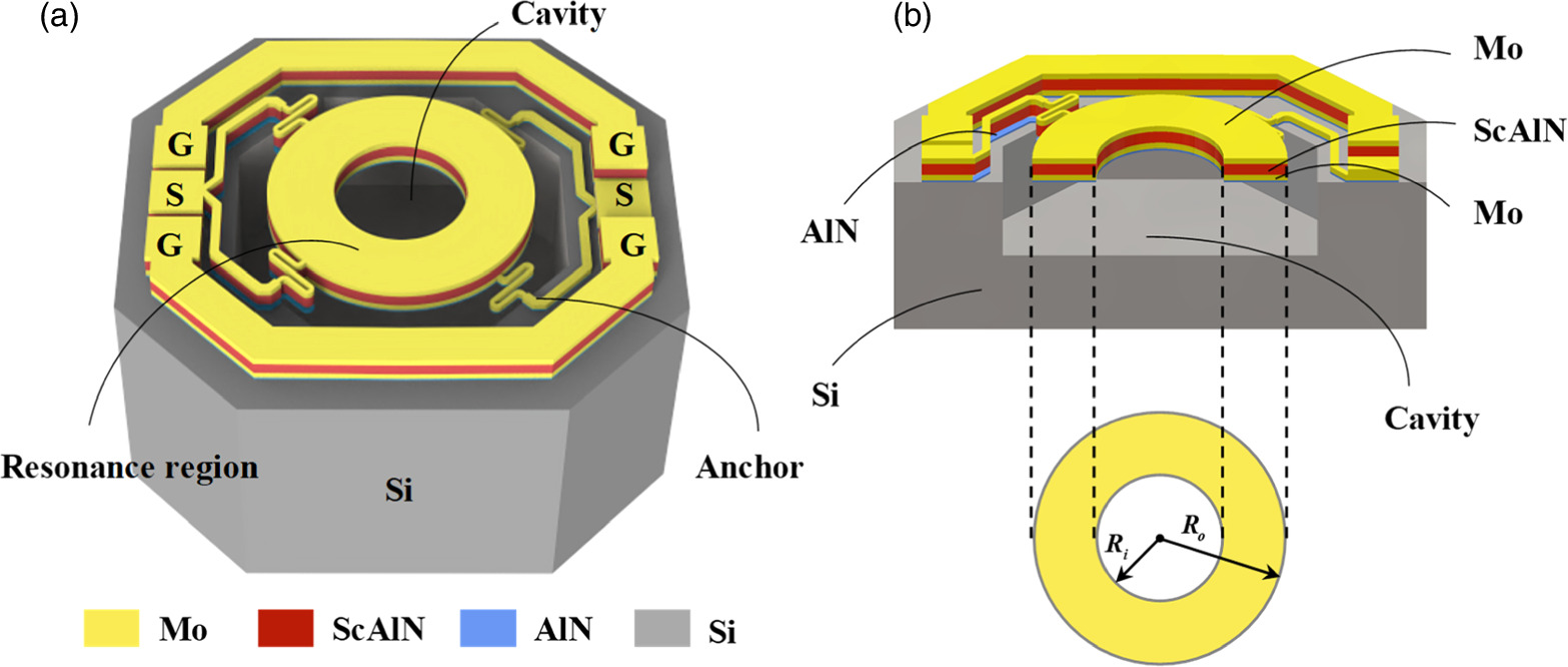
Fig. 1. The schematic diagram of the ring resonator. (a) Three-dimensional diagram, included the silicon substrate with a cavity, the resonance region, the G-S-G pads and anchors. (b) The cross-section diagram of the ring resonator consisting of Mo-Sc0.2Al0.8N-Mo layers, and the plane view of the resonance region.
Download figure:
Standard image High-resolution imagePiezoelectric devices exhibit specific vibration modes known as eigenmodes during free vibration, which are determined by the internal medium and structure of the device. Eigenmodes include fundamental modes and higher-order modes, corresponding to different frequencies and vibration shapes. Modal analysis of piezoelectric devices is critical to understanding vibration characteristics and response at specific frequencies. It is fundamental for designing device structures and optimizing performance.
In this letter, a three-dimensional model of a ring resonator was established using the COMSOL software. The first six fundamental modes of the resonator, 19) ranging from low to HF, were analyzed and presented in the Fig. 2, with scale bars indicating the displacement amplitude of the piezoelectric thin film.
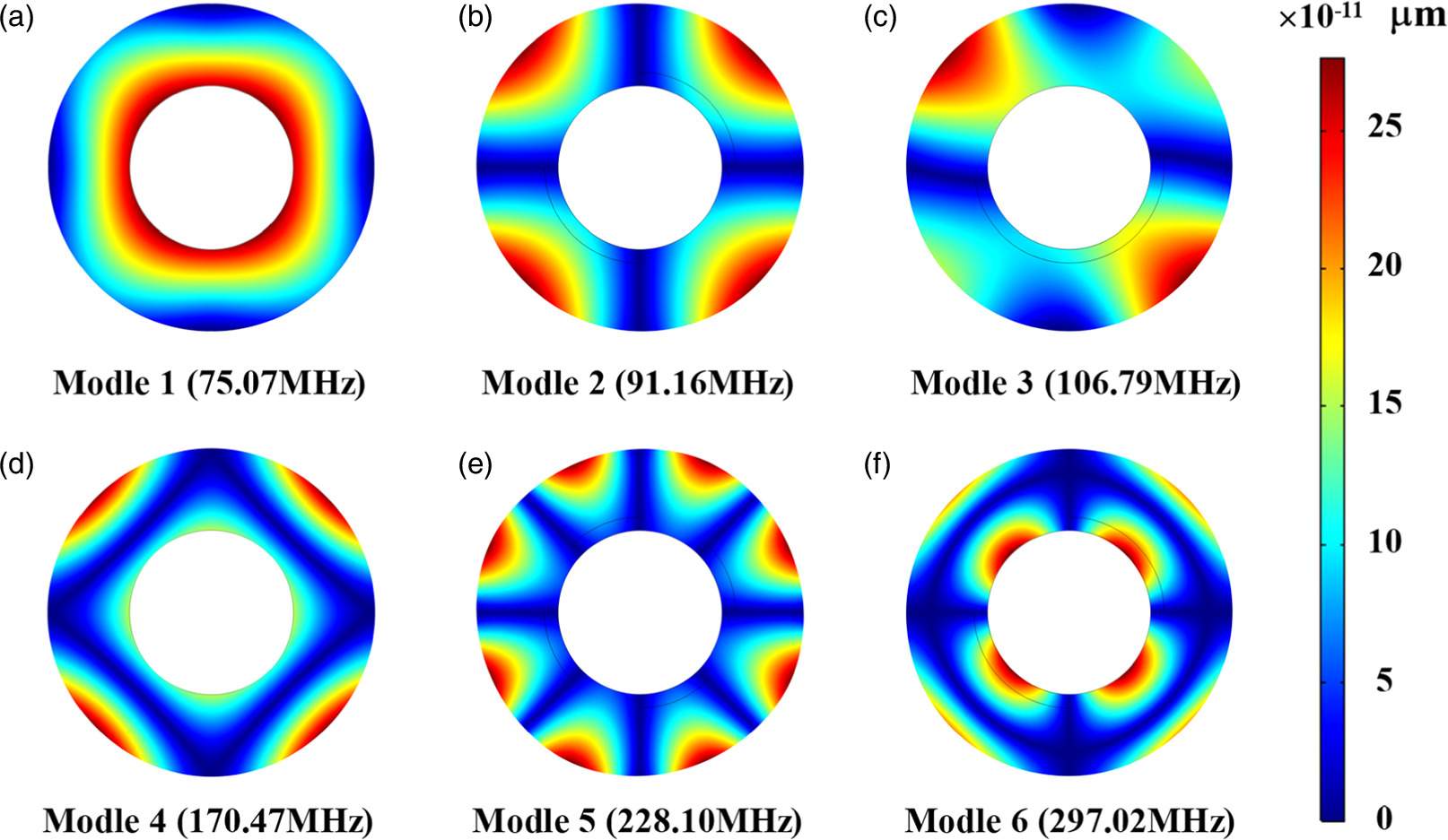
Fig. 2. The first six fundamental modes of the ring piezoelectric resonator.
Download figure:
Standard image High-resolution imageHigher-order modes refer to the eigenmodes of the piezoelectric resonator that have frequencies higher than the fundamental modes. These modes can affect the response and stability of the device, especially when resonance occurs near the operating frequency. Therefore, in the design and optimization of piezoelectric resonators, the higher-order modes also need to be analyzed and considered to ensure the device's performance within the operating frequency range. Figure 3(a) is the impedance curve of the ring resonator.
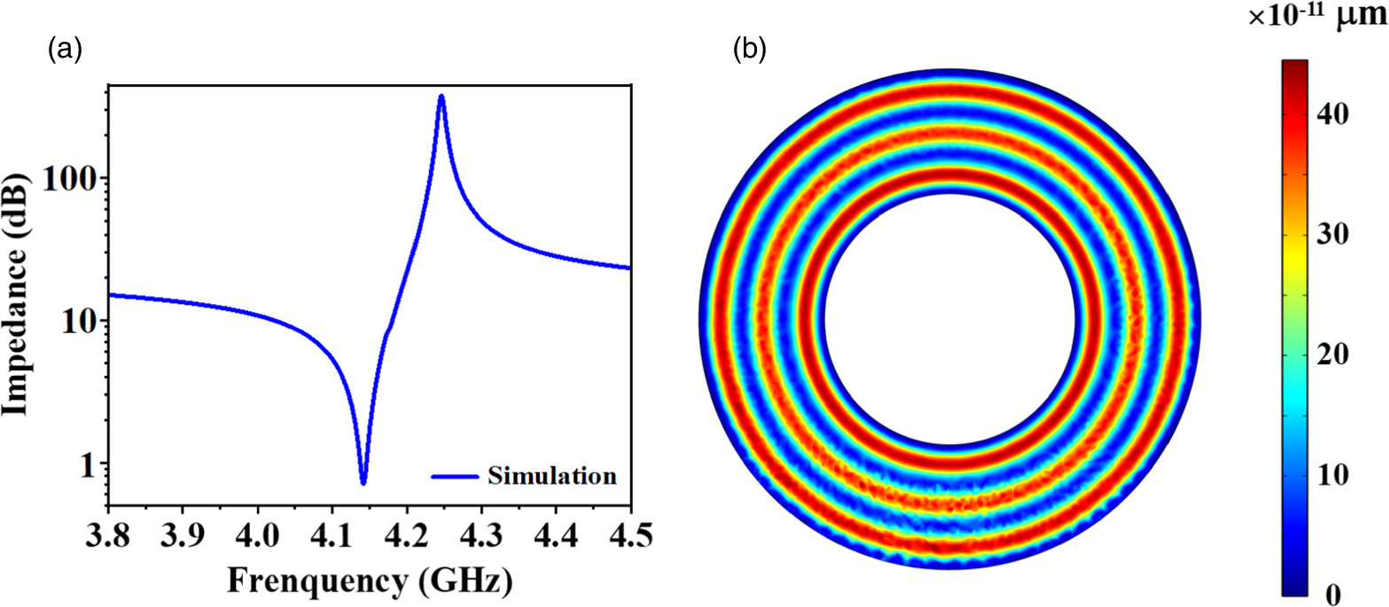
Fig. 3. The simulation results of the ring resonator by COMSOL. (a) The impedance curve of the ring resonator. (b) Higher-order vibration mode of the ring resonator.
Download figure:
Standard image High-resolution imageFigure 3(b) displays the higher-order vibration mode of the simulated ring resonator in this study. When an electric field is applied in the thickness direction, it causes expansion or contraction along the radial direction of the ring.
According to Ambati et al., 15) the frequency equation of a ring vibrating in a pure radial-extensional mode shape is expressed as:
where

J and Y are the first and second Bessel functions, respectively, while M and N are the modified Bessel functions. This can accurately calculate the frequency, but the formula is complicated. When the average radius of the ring ( ) significantly exceeds its width (Wr
), the vibration modes of the ring can be effectively approximated as those of a bar vibrating along its length. The length and width of the bar can be equivalent to the width and average perimeter of the ring respectively.
20) The frequency of the ring resonator can be calculated using the following formula
12)
) significantly exceeds its width (Wr
), the vibration modes of the ring can be effectively approximated as those of a bar vibrating along its length. The length and width of the bar can be equivalent to the width and average perimeter of the ring respectively.
20) The frequency of the ring resonator can be calculated using the following formula
12)

where Wr
is the width of the ring-shaped resonant body (i.e., subtract inner radius of the ring from outer radius of the ring) and is fixed 60 μm in all the MEMS resonators in this research,  is the effective Young's modulus, σ is the Poisson's ratio and
  is the effective mass density of the composite structure materials. According to formula (1), the resonant frequency is mainly determined by the width of the ring. Hence, by adjusting geometric parameters like the ring's length, width, inner, and outer radius, it's possible to modify the resonator's physical characteristics, thus influencing its resonant frequency. This approach enables the fabrication of resonators with varying frequencies from a single wafer, catering to the specific requirements.
Table I shows the geometric parameters of the resonator, including the thickness of each layer of material and the size of the inner and outer radius.
Table I. Geometric parameters of the resonator.
| Thickness (nm) | |||||
|---|---|---|---|---|---|
| Parameters | Top Mo | Sc0.2Al0.8N | Bottom Mo | Rin (μm) | Rout (μm) |
| Value | 136 | 540 | 144 | 60 | 120 |
The primary steps involved in the fabrication of a ring resonator are depicted in Fig. 4. The process begins with etching a cavity into a silicon substrate. Next, the SiO2 is deposited as a sacrificial layer and the surface is flattened using chemical mechanical polishing (CMP). To improve the quality of piezoelectric film, a 35 nm AlN is deposited as a seed layer followed by the deposition of Mo and Sc0.2Al0.8N layers. A 144 nm layer of Mo is then sputtered and patterned to form the ring bottom electrode. Sequentially, a 540 nm Sc0.2Al0.8N piezoelectric layer and a 136 nm top Mo electrode layer are deposited by sputtering, and patterned to form a ring-shaped structure. Finally, the sacrificial layer is etched using vapor hydrofluoric acid (VHF) to release the device.
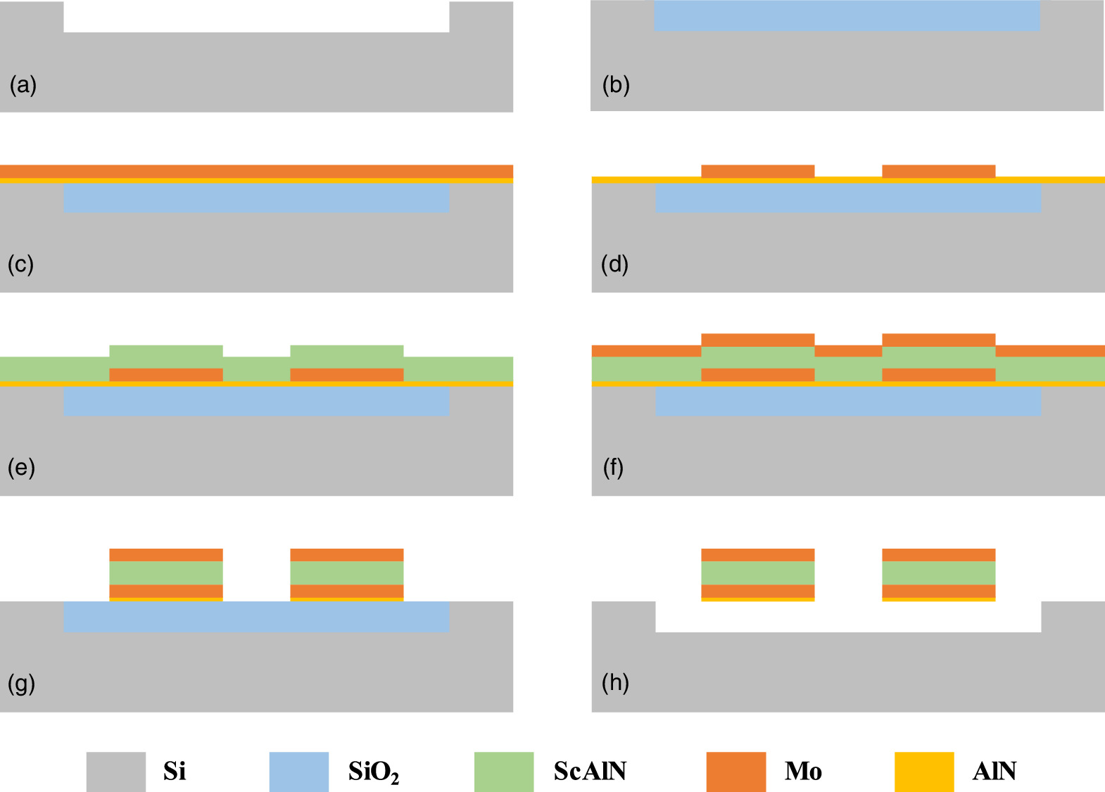
Fig. 4. Main process steps of the fabrication of ring resonator. (a) Forming cavity by etching the Si substrate. (b) SiO2 deposition and CMP. (c) AlN seed layer and bottom Mo deposition. (d) Bottom Mo pattern. (e)–(g) Sc0.2Al0.8N and top Mo deposition and pattern. (h) Releasing the cavity by VHF.
Download figure:
Standard image High-resolution imageFigure 5 illustrates the scanning electron microscopy (SEM) schematic diagram of the fabricated device. As shown in Fig. 5(a), the electrode morphology matches the anticipated specifications, exhibiting a smooth and unblemished surface. Figure 5(b) illustrates the sandwich structure comprising Mo-Sc0.2Al0.8N-Mo layers with thicknesses of 136 nm-540 nm-144 nm and a 35 nm AlN seed layer.
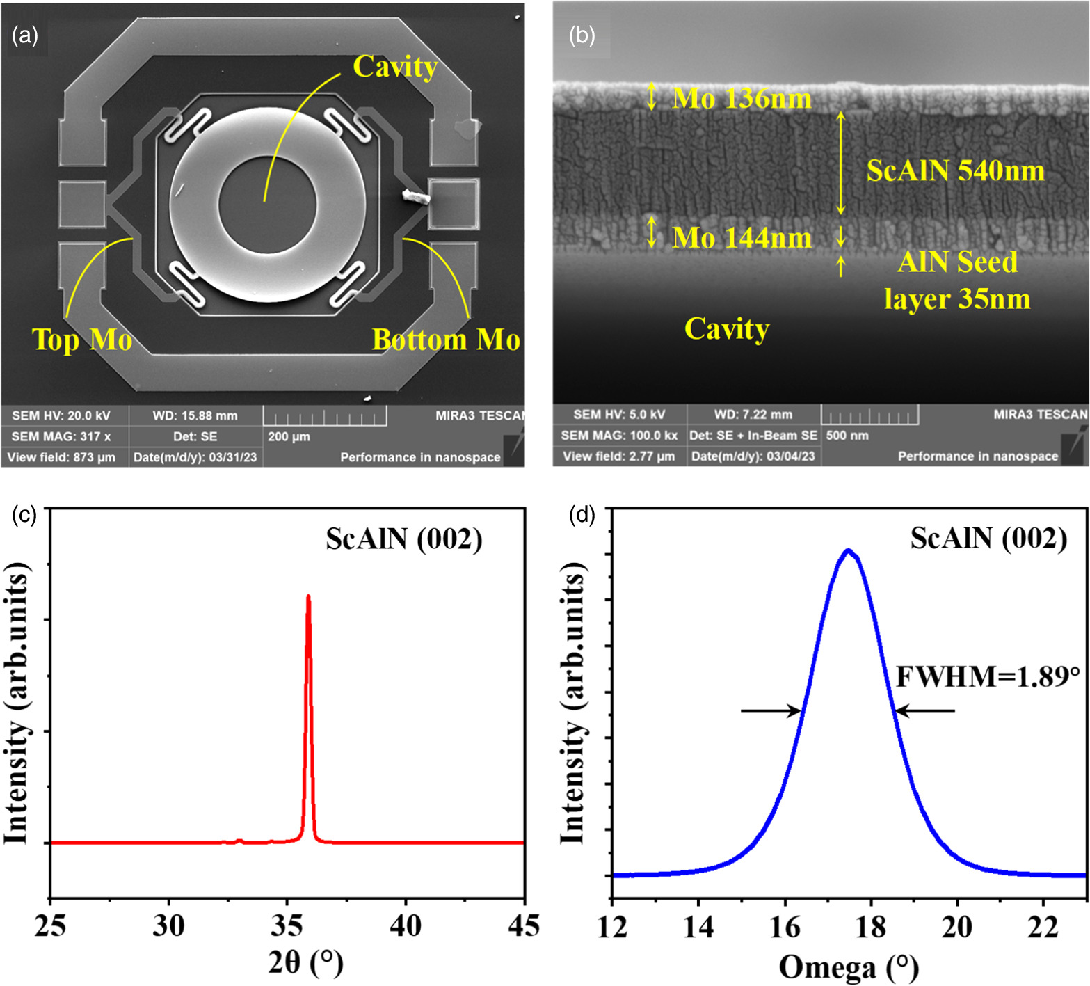
Fig. 5. SEM image of the fabricated ring resonator and characterization of the Sc0.2Al0.8N film. (a) Optical microscope of the fabricated ring resonator. (b) SEM image of the cross-section view of the fabricated ring resonator. (c) XRD pattern of the Sc0.2Al0.8N. (d) XRD rocking curve of Sc0.2Al0.8N.
Download figure:
Standard image High-resolution imageIn the X-ray diffraction (XRD) of Fig. 5(c), there is a prominent diffraction peak at the 002 orientation, which indicates that Sc0.2Al0.8N has a single out-of-plane orientation. The crystallinity of the Sc0.2Al0.8N films was evaluated through a rocking curve test, which revealed a full width at half maximum (FWHM) of 1.89°. This observation indicates the films possess good crystallinity, a crucial factor influencing the device's performance. A well-ordered and high-quality crystal structure within the films ensures their effectiveness in fulfilling their intended functions within the device.
The MBVD equivalent circuit model of the resonator is shown in Fig. 6(b), which increases the dielectric loss of the piezoelectric layer and the resistive loss of the electrode layer, providing a convenient method to obtain the electrical parameters of the resonator. The model consists of the following six components: C0 is the static capacitance, R0 is the dielectric loss of the piezoelectric film, and Rs is the electrode lead loss. Cm , Lm , and Rm represent mechanically related dynamic capacitance, dynamic inductance, and loss, respectively.
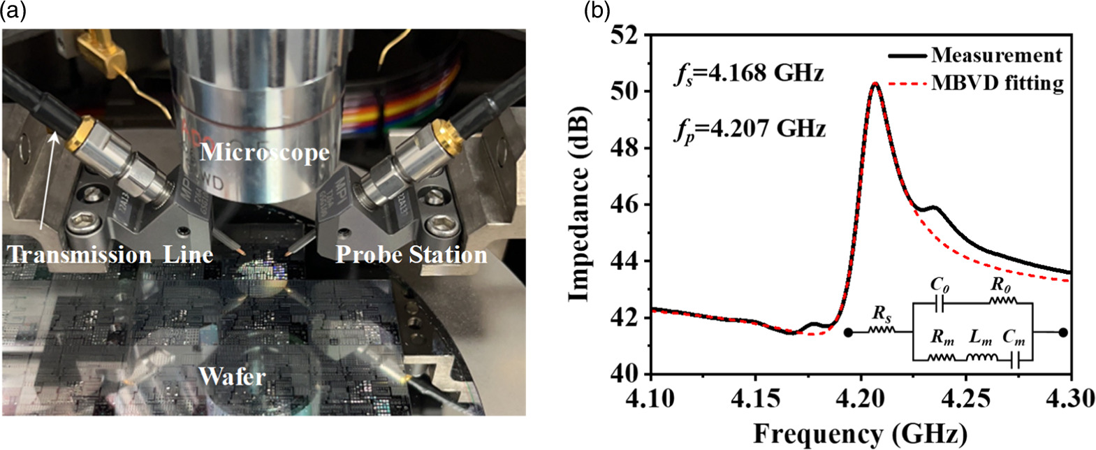
Fig. 6. Experimental results of the ring resonator. (a) Probe station measurement system, including microscope, probe and transmission line. (b) MBVD equivalent circuit, and the measured and MBVD fitted plot for ring resonator.
Download figure:
Standard image High-resolution image
These can be calculated by the following formula: 12)


where  is the relative dielectric constant of Sc0.2Al0.8N, w is the ring width (
 ),
),  is the average radius of the ring, t is the thickness,
  is the equivalent Young's modulus of Sc0.2Al0.8N,
  is the piezoelectric coefficient, σ is the Poisson's ratio of Sc0.2Al0.8N,
  is the quality factor, and
  is the unloaded center frequency, respectively. The Rm
-Cm
-Lm
of circuit branch reflect the interaction between RF signals and acoustic waves. The series frequency
is the unloaded center frequency, respectively. The Rm
-Cm
-Lm
of circuit branch reflect the interaction between RF signals and acoustic waves. The series frequency  of the resonator can be expressed in terms of Lm
and Cm
, and the parallel frequency
of the resonator can be expressed in terms of Lm
and Cm
, and the parallel frequency  can be expressed in terms of Lm
, Cm
and Rm
. The formula is as follows:
21)
can be expressed in terms of Lm
, Cm
and Rm
. The formula is as follows:
21)


From Fig. 6(b), it can be seen that the resonance frequency of the resonator is 4.168 GHz and the anti-resonance frequency is 4.027 GHz, according to this equation: 22)

 is calculated with a value of 2.3%.
On the other hand, by fitting the MBVD model with the impedance curve obtained from experimental measurements, the electrical parameters of the resonator such as Lm , Cm and Rm can be extracted, thereby obtaining an accurate representation of the electrical behavior of the resonator.
The devices were characterized using a Keysight N5222B network analyzer. In order to reduce the measurement error, a standard transmission line was utilized to connect the probe station system to the network analyzer, as shown in Fig. 6(a). This setup allowed for precise analysis of the devices' electrical characteristics, including impedance, resonance frequency, and quality factor. The characterization process involved setting up the frequency range and scan step, followed by a short-load-open-through standard calibration to further enhance the accuracy of the test. During the measurement process, a two-port probe was connected to the G-S-G pads of the device, as shown in Fig. 1.
Figure 6(b) shows the measured impedance curve of the device in the frequency range of 4.1 ∼ 4.3 GHz. The experimental results are in high agreement with the simulation results. In addition, the extracted electrical parameter values of the resonator are shown in Table II. These parameter values reflect the characteristics and performance of the resonator, which are helpful for further analysis, optimization and integration into practical applications.
Table II. MBVD model parameters.
| MBVD model | Rm (Ω) | Cm (pF) | Lm (nH) | C0 (pF) | R0 (Ω) |
|---|---|---|---|---|---|
| Value | 38.240 | 0.0028 | 502.252 | 0.407 | 2.81 |
This study presented the design and fabrication of a piezoelectric ring resonator featuring a Sc0.2Al0.8N film with an exceptional C-axis orientation, characterized by a narrow FWHM of 1.89°. The manufacturing process involved multiple steps, including coating, lithography, etching, and cavity release. The fabricated resonator was characterized and tested using SEM and probe station measurement system. Subsequently, MBVD equivalent circuit model was established and fitted to the measured results, facilitating the precise extraction of electrical parameters. The resonance frequency of the resonator is 4.168 GHz and the anti-resonance frequency is 4.207 GHz, with the  measuring at 2.3%. This work provides a theoretical foundation for the design of HF ring resonators through comprehensive theoretical analysis, manufacturing, and characterization.
Acknowledgments
This work was supported by the Young Scientists Fund of the National Natural Science Foundation of China under Grant 62204177, and the Fundamental Research Funds for the Central Universities under Grants 2042022kf1027 and 2042023kf0218, Open Fund of Hubei Key Laboratory of Electronic Manufacturing and Packaging Integration (Wuhan University) under Grant EMPI2023025. The authors would like to thank the Core Facility of Wuhan University and the School of Power and Mechanical Engineering of Wuhan University for access to analytical equipment.