
Abstract
It is expected that the operation of microwave kinetic inductance travelling wave parametric amplifiers (KITWPAs) can be extended to the millimetre (mm) and the sub-mm wavelength range as long as the frequency is below the gap frequency of the superconducting film. This paper presents possible mm-wave designs for KITWPAs based on microstrip transmission lines. Our device is designed based on the BCS (Bardeen–Cooper–Schrieffer) model which successfully reproduces the measured transmission profile, gain, bandwidth, and nonlinear response of a fabricated KITWPA operating in the Ka-band, and includes the millimetre-wave dielectric loss determined by fitting the quality factor of a W-band microstrip resonator. We suggest a layout for a KITWPA operating near 220 GHz that can be fabricated using the same superconducting properties as the Ka-band device and can be coupled to a waveguide system. We conclude the paper by extending the 220 GHz design to higher frequency regimes approaching 1 THz.
Export citation and abstract BibTeX RIS

Original content from this work may be used under the terms of the Creative Commons Attribution 4.0 license. Any further distribution of this work must maintain attribution to the author(s) and the title of the work, journal citation and DOI.
1. Introduction
It is well known that reducing the noise temperature of the first stage detector in an astronomical heterodyne instrument would have a huge impact on the overall system noise temperature of the receiver since any loss introduced by the detector would be cascaded and compounded down the line. This is best illustrated with the system noise temperature equation:  , where Gdet, GLNA, Tdet, TLNA & TIF are the gain and temperature of the first stage detector, the readout low noise amplifier (LNA) and the IF chain respectively [1]. Here,
  represents the loss of the RF passive optical components of the receiver chain. The first stage detector generally are in the form of Superconductor–Insulator–Superconductor (SIS) or HEB (Electron Bolometer) mixers for the millimetre (mm) and sub-mm instruments [2]. It is clear that the conversion loss or gain of these first stage detectors affects the noise contributions of all the components along the chain. Therefore, a quantum-noise limited pre-amplifier with high gain before the mixer stage (
 ) would improve the receiver sensitivity significantly. Although there are existing semiconductor amplifiers that demonstrate operation in the mm range [3–5], their noise performance is still far from the fundamental limit. Therefore, to date, most if not all of the high-frequency heterodyne receivers in the mm/sub-mm and terahertz (THz) regimes still operate without a pre-amplification stage, unlike radio/microwave receivers which utilise LNAs as the first stage detector.
Recent developments in ultra-low noise, wide band amplifiers using superconducting thin film technology [6–10] could potentially change the scenario and be deployed as the needed pre-amplifier for mm/sub-mm/THz receivers. However, since the first report of the kinetic inductance travelling wave parametric amplifier (KITWPA) [6] about a decade ago, most of the KITWPA development is still focusing on operating in the microwave range below 20 GHz; apart from a few that went above that range into the low mm wavelength range [11] and up to a maximum of W-band [12]. In theory, a KITWPA would still be functional as long as the operational frequency range of the device is below the gap frequency of the high kinetic inductance thin film used to fabricate the amplifier. This suggests the exciting prospect of a quantum-noise-limited amplifier that can operate in the mm/sub-mm & THz regime, a task seemingly too challenging for conventional semiconductor amplifier technology.
KITWPAs are based on transmission line structures fabricated using conventional photo-lithography or e-beam techniques used for producing most mm/sub-mm/THz devices. Since the scale of the transmission line features can easily be made much smaller than a wavelength even up to about 1 THz, it should be straightforward to scale the microwave designs to the higher frequency regime. As they are based on similar materials, a KITWPA pre-amplifier could be integrated on-chip with the detector circuits in the near future, forming a compact receiver configuration that can be installed on existing facilities with minimum disruption to the infrastructure. The pump power required to operate a KITWPA is around three orders of magnitude lower than the typical bias power needed for conventional semiconductor amplifier technology, so arrays may be deployed without excessive burden on a cryogenic cooler. The operational bandwidth of the microwave KITWPA can be quite large and is limited by the engineered dispersion of the device that prevents the phase matching of nonlinear processes (e.g. pump's third harmonic generation) apart from parametric amplification. At higher operating frequencies, particularly as the gap frequency is approached, the variation of the surface inductance with frequency adds intrinsic dispersion to the superconducting transmission line. The phase mismatch produced by this dispersive effect will limit the bandwidth of the KITWPA. We show in the following sections that the bandwidth can remain quite high, particularly compared to what can be achieved with near quantum-limited heterodyne receiver systems.
While microwave KITWPAs have been produced using both coplanar waveguide (CPW) and microstrip transmission line geometries, the latter design is more readily adaptable to mm-wave applications because of the tendency of CPW to radiate at high frequency, so we adopt a microstrip-based design for this study. In section 2.1, we use the measurements of the Ka-band KITWPA described in Shu et al [11] to establish the superconducting parameters of the NbTiN (niobium titanium nitride) microstrip line, used later for the mm-wave KITWPAs. Section 2.2, extrapolates those results to higher frequency using the Mattis–Bardeen expressions [13] for the frequency-dependent complex conductivity. Section 2.3 discusses the mm-wave dielectric loss, which is explored by fitting the response of a W-band microstrip resonator. In section 3, we discuss a method for coupling the devices in a mm-wave environment using waveguide probes and present a design for a mm-wave KITWPA covering bands 5 and 6 of ALMA (Atacama Large Millimetre/sub-millimetre Array). Finally, in section 4, we discuss the material-dependent upper limit of operating such KITWPA near its gap frequency.
2. Estimation of mm-wave material parameters
2.1. Surface impedance recovery
We constrain the superconducting material parameters for use in our model by fitting the measured 'unpumped' S21 transmission spectrum of our Ka-band device [11]. That device was fabricated based on a transmission line with the periodic structure depicted in figure 1. The central microstrip line is shunted with a series of open stub sections, the length of which is modulated to produce a stopband in the transmission spectrum around 38 GHz, as shown in figure 2. The location of the stopband depends sensitively on the superconducting properties. Both the central microstrip line and the stub sections were formed using a 250 nm wide, 35 nm thick NbTiN conductor layer, which is deposited and patterned on a 100 µm thick high-resistivity silicon substrate ( 11.9). A 60 nm amorphous silicon (aSi,
  10.3) dielectric layer deposited on top of the conductor. Finally, a 200 nm NbTiN 'sky-plane' layer is deposited to form an inverted microstrip geometry.
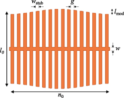
Figure 1. The notations that define the critical dimensions of the unit cell of continuous impedance modulating inverted microstrip structure that made up the entire Ka-band KITWPA.
Download figure:
Standard image High-resolution image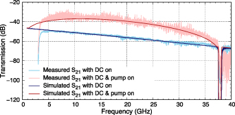
Figure 2. The shift in the stopband's position is caused by the additional kinetic inductance gained through the applied DC current. Correcting the surface kinetic inductance with the expected DC current value resulted in the same magnitude of the shift in the stopband's frequency. Applying an additional RF pump tone at 38.8 GHz with an amplitude of −27.5 dBm successfully recovers the measured gain profile, not only the peak gain but the shape and bandwidth as well.
Download figure:
Standard image High-resolution imageWe modeled the device using a commercially available 3D electromagnetic simulator Ansys® high-frequency structure simulator (HFSS), with exactly all the dimensions and topology listed in [11] and BCS functions built into the simulations. The latter is performed by applying the Mattis-Bardeen surface impedance as impedance boundary condition on the perfect conductor modelling the transmission line [14, 15]. For completeness, we listed all the dimensions of the inverted microstrip structure used for the simulation in table 1 with reference to figure 1. The NbTiN film is expected to have a critical temperature of  K, corresponding to a gap parameter
  meV, given a ratio
  [16], which is slightly high than the weak coupling BCS value. The normal state resistivity
  cm [11].
Table 1. The critical dimensions of the inverted microstrip structure used to form the unit cell and the entire Ka-band TWPA.
| w | g |

| l0 |

| No. of | Total no. |
|---|---|---|---|---|---|---|
| (nm) | (nm) | (nm) | (µm) | (µm) | stubs, n0 | of cells |
| 250 | 500 | 250 | 6 | 0.1 | 51 | 550 |
However, if we used the expected film parameters, we found that the theoretical model would poorly predict the behaviour of the measured S21 spectrum; the stopband position would be off by several GHz. To match the stopband position, we can either retain the normal state resistivity of the NbTiN film as estimated in Shu et al [11], but vary the gap voltage from the designated 4.1 meV; or retain that estimate but varying ρ (all other parameters are well constrained in our fabrication process). In either case, we are simply adjusting the surface inductance per square value to match that of the actual film. The reason behind the former consideration is that the  was measured in an experimental setup where the temperature sensor was anchored at the sample holder, and we expect that the device chip may be at a warmer temperature than the measured 12.5 K; while the latter related to the uncertainties in measuring the actual ρ of the film across the entire wafer. Although not shown in figure 2, if we adjust ρ to 168
  cm (with
  remaining at 12.5 K), the simulated transmission curve would match the position of the stopband extremely well, as well as the width of the stopband too. Similarly, if we adjust the
  to 15.0 K but retain ρ at 200
  cm. In reality, the actual surface impedance could be at any value between the two limits (ρ = 168–200
  cm &
cm &  –15.0 K).
As our KITWPA device is designed to operate in the DC-biased 3-wave (DC3WM) mixing regime, it is obvious that the stopband position would shift when a DC current is applied. Using the recovered surface impedance value from above (here we use only the case where  cm and
  meV), we managed to match the measured transmission curve when DC current is applied accurately by simply multiplying the surface inductance calculated by the BCS (Bardeen–Cooper–Schrieffer) and Mattis–Bardeen equation, by the expected nonlinear inductance i.e.
 ![$L_{\mathrm{k}} = L_{0}\times[(1+({{I_{\mathrm{dc}}}}\!/\!{{I^*}})^2+({{I_{\mathrm{dc}}}}\!/\!{{I^{*^{{\prime}}}}})^4]$](https://content.cld.iop.org/journals/0953-2048/37/3/035006/revision2/sustad20fdieqn21.gif) where
where  mA and
  2.8 mA, with the DC current applied at 0.57 mA, as indicated in [11], and shown in figure 2, without including the BCS surface resistive loss from the device. In practice, the quartic term is typically negligible compared to the qudratic term due to the critical current of the device,
  . Note that the simulated curves in figure 2 were made by taking into account the 50 dB attenuation (from various stages of attenuators installed in the line in the experiment), and the frequency-dependent attenuation of the RF cables measured experimentally at 0.098 dB GHz−1 m−1 (or 0.49 dB GHz−1) [12].
Once we obtain the DC-biased transmission curve, it is straightforward to simulate the gain curve. Here, we use our coupled-mode equation (CME) model as presented in [17] but modified to operate in the DC3WM mode. As shown in figure 2, we successfully recover a gain curve that matches very well with the measurement, not only the level of gain but the bandwidth and the overall gain-bandwidth profile. The RF pump frequency was set at 38.8 GHz with an amplitude of −27.5 dBm as indicated in the experiment. We stress that in our model, we do not alter any parameters other than recovering the actual surface reactance via ρ.
2.2. High frequency surface impedance
Adopting the values for the normal metal resistivity and the gap parameter adopted above, the surface impedance  may be found using the Mattis–Bardeen expressions for the complex conductivity
  [13]. The integral expressions for
  are valid up to the gap frequency, beyond which the attenuation jumps abruptly, as photons beyond that energy are able to directly break Cooper pairs. For the device designs considered here, the film thickness t is much less than the penetration depth, so the current is nearly uniform through the film and the thin film limit is valid. In this case, the surface impedance is
from which we can calculate the loss and propagation velocity of an NbTiN microstrip line as a function of frequency. For the geometries of interest for our KITWPA, the Pearl length  , which is the length scale over which the current varies laterally across the film [18], is much longer than the microstrip conductor width, w. In this case, the current is uniform across the microstrip conductor, and the inductance per unit length can be written in terms of a sum of magnetic and kinetic contributions as
  , where
  is the inductance associated with the magnetic field,
  is the surface inductance of the ground plane and wgp
is the effective width of the current distribution in the ground plane [12]. Due to the large kinetic inductance of NbTiN and narrow geometry of the microstrip,
is the surface inductance of the ground plane and wgp
is the effective width of the current distribution in the ground plane [12]. Due to the large kinetic inductance of NbTiN and narrow geometry of the microstrip,  , and the ground plane contribution is also small in comparison to the conductor's inductance as the ground plane currents are spread over a much wider area. The propagation velocity
  and characteristic impedance
  can be found using an expression [19] for the capacitance per unit length of a microstrip line. The power attenuation constant is then given by
  or
or  in terms of dB per wavelength. These quantities are plotted as a function of frequency in figure 3. Interestingly, for a fixed number of wavelengths, the loss due to the surface resistance stays roughly constant through the mm-wave region at a very low level before increasing abruptly at the gap frequency. Nevertheless, the propagation velocity shows dispersion due to the frequency dependence of σ2, varying more rapidly as the gap frequency is approached, hence may be more of a concern for mm-wave operation, which we shall address later. We note that the behavior very near the gap frequency may be somewhat different from that shown in the figure due to disorder induced broadening of the singularity in the quasiparticle density of states near the gap energy [20]. That effect would be expected to smear the abrupt onset of increased dissipation and slightly lower the maximum frequency of the KITWPA. Another source of broadening of the density of states singularity is effect of the current associated with the strong RF pump tone used to drive the KITWPA [21]. Generally for KITWPAs, including for the designs considered later in this report, the nonlinearity at the operating point is relatively weak, resulting in only a percent level effect.
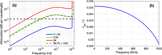
Figure 3. Left: calculated millimeter-wave attenuation of a 1 µm wide, 35 nm thick NbTiN microstrip line with a 60 nm thick aSi dielectric. The attenuation due to metal loss is shown from 2–3 K for films with  meV and
  cm (solid lines), and the reduced 3 K attenuation in a film with
  K (
K ( meV) is shown with the dashed red line. The dielectric loss, assumed here to be frequency independent, corresponds to the resonator measurement (figure 4). The frequency variation of the propagation velocity in the same microstrip line. The propagation velocity is low due to the large kinetic inductance.
Download figure:
Standard image High-resolution image2.3. High frequency dielectric loss
In the previous Ka-band KITWPA analysis, we did not include the effect of loss tangent of the dielectric, which could potentially be important at high frequencies. To investigate the high-frequency dielectric loss, we conducted a separate experiment where we measured the resonance curves of W-band half-wavelength microstrip resonators fabricated using the same processes and film stack-up as the Ka-band KITWPA. The chip containing the resonators was designed to fit in a split-block waveguide machined from copper (see figure 4). E-plane waveguide probes on either end of the chip were utilized to couple power between the WR-10 waveguides and an on-chip 1 µm wide microstrip line. The resonators are formed with 'U' shaped sections of the same microstrip line and are gap-coupled to the readout line. The resonators have total lengths between 33 and 57 µ, corresponding to resonance frequencies in the W-band, given a propagation velocity close to that shown in figure 3.
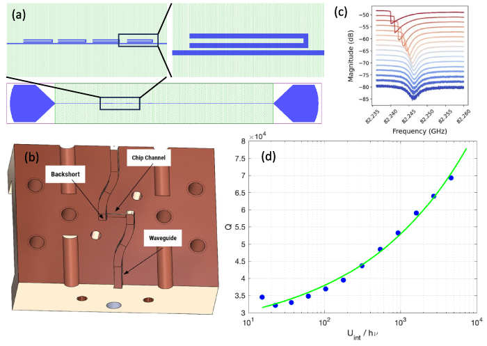
Figure 4. (a) Layout of the W-band microstrip resonator test chip. (b) One-half of the split block housing with WR-10 input/output waveguides. The resonator chip is glued into the channel between the waveguides. (c) Measured transmission curves for one of the resonators for various excitation powers, increasing from blue to red in steps of 2 dB. (d) Extracted internal Q-values versus resonator stored energy in photons.
Download figure:
Standard image High-resolution imageThe transmission S21 parameters of the resonators were measured using a vector network analyzer with W-band waveguide extenders. The transmission curves for one resonator, measured at 0.9 K, are shown in figure 4(c) for a range of excitation powers. For the higher excitation powers, the resonances are distorted due to the nonlinear kinetic inductance and evolve into the characteristic shape of a Duffing resonator. The internal loss versus the energy stored in the resonator is extracted by fitting to a nonlinear resonator model [22] and is shown in figure 4(d) as a function of Uint, the energy stored in the resonator, which is determined from the excitation power Pin through
where ωr and Qr are the frequency and the quality factor of the resonator respectively, and Qc is the coupling factor. The decrease in Q at low power is the expected behavior of loss due to two-level-systems (TLS) [23] in the aSi dielectric and is described by the standard TLS model. For a KITWPA, the limiting low-power value of the loss is of interest, which we estimate by fitting the data to the equation

where Uc
is the critical energy above which there is a power dependence to the quality factor. The parameter φ used in the standard TLS theory is 0.5, but lower values have been found for low-loss amorphous dielectrics [24], so we include it as a fitting parameter. The fit, shown in the figure 4(d), suggests that  and φ = 0.31. The power attenuation due to dielectric loss in a transmission line of length l is
  , where
  is the propagation constant, and
  is the loss tangent. Expressed in dB, the loss is
  dB per wavelength, which is relatively small given that the length of a KITWPA is on the order of a few hundreds of wavelengths, resulting in minimal excess noise or heating from the applied pump. Nevertheless, for subsequent analysis in the mm-wave range, we include this dielectric loss in all our models.
3. Designs of mm-wave KITWPA
With the recovered surface impedance above, we can now design a realistic dispersion-engineered mm-wave NbTiN KITWPA with optimized high-gain operation. In the following analyses, we assume  cm and
  meV, and aim for operating near 220 GHz. While our Ka-band KITWPA operated in a 3-wave mixing (3WM) mode, we base our higher frequency designs on 4-wave mixing (4WM). The two mixing modes are often similar in terms of practical performance and underlying mechanisms, but 4WM designs offer several advantages particularly at higher frequencies [12]. This choice simplifies the design, particularly in the case where the KITWPA will operate in a waveguide environment, as a DC-biased 3-wave device would require the injection of a DC current through an on-chip bias tee structure as well as a pump at approximately twice the signal frequency, which would need a different-sized waveguide that may not be feasible in practice.
3.1. Power coupling at high frequencies
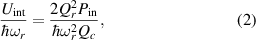
For operation in mm/sub-mm wavelength, apart from the dielectric loss, there are several design considerations that need to be taken into account e.g. it is most likely that the device will have to be coupled using a waveguide feed [25] instead of the commonly used coaxial cables at microwave regime such as SMA or SMK cables. Therefore, the characteristic impedance of the TWPA need not be restricted to firmly 50 Ω, but should be optimised to match the output impedance of the feeding antenna. Furthermore, the choice of substrate used to support the TWPA becomes a crucial issue. For most waveguide antennas, such as the probe antenna [25] (the most commonly used antenna in this frequency range), a thinner substrate with a lower dielectric constant is preferable such that it does not load the waveguide and supports unwanted substrate modes.
One potential solution to this is to use a membrane technology such as silicon-on-insulator or silicon nitride where only the silicon handle layer underneath the antenna is etched away to form the membrane but retain the handle to support the remaining TWPA circuit. Nevertheless, to avoid the need for sophisticated fabrication technology, we opt for a simpler solution by fabricating the device on top of a thin 40 µm quartz substrate with  . Figure 5 shows the optimised design of the feeding antenna embedded inside a
  mm rectangular waveguide with a cutoff frequency near 150 GHz. The overall device makes use of two of these antennas, one at either end of TWPA, as was done for the W-band resonator measurement device depicted in figure 4. The dimensions of the probe antenna with an optimised output impedance of 67.7 Ω, and the supporting substrate, are tabulated in table 2. As can be seen in figure 5, our probe antenna can achieve close to 0 dB coupling from 170–300 GHz, broad enough to cover the bandwidth of our TWPA.
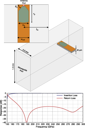
Figure 5. (Top) The image illustrates the design of the probe antenna with arc,  , width,
  and taper angle, θp. The distance from probe center line to backshort is lbs and the substrate width is wsub. (Bottom) The insertion and return loss performance of the probe antenna, which covers an operational frequency range from 170–300 GHz. The probe antenna was optimised using the same critical parameters of the NbTiN film used to form the mm-wave KITWPA.
Download figure:
Standard image High-resolution imageTable 2. The critical dimensions of the probe antenna with an output resistance of 67.7 Ω.

|

|

|

|

|
|---|---|---|---|---|
| (µm) | (µm) | (µm) | (µm) | (°) |
| 235 | 135 | 155 | 326.75 | 50.7 |
3.2. 220 GHz millimetre-wave KITWPAs
In this section, we present the design of the mm-wave TWPA that matches the output impedance of the probe antenna using the same substrate and thin film technologies. Here, we retain most of the dimensions used to construct the Ka-band TWPA presented above, except the unit cell length that is adjusted to operate near 220 GHz, the stub's length, and the gap between the stubs modified to match 67.7 Ω, and the stub length modulation calibrated to achieve good phase-matching in the designated frequency band range. The optimized dimensions of the TWPA are tabulated in table 3, and the predicted gain profile of the device is presented in figure 6, while figure 7 illustrates the layout of the entire mm-wave TWPA chip together with the input/output probe antennas, connected to two rectangular waveguides for signal coupling at high frequency.

Figure 6. (a) The gain-bandwidth profiles of the mm-wave KITWPA, pumped with  at 216.35 GHz. (b) The transmission profile and nonlinear dispersion of the TWPA without the probe antenna. At the third pump's harmonic frequency, the large nonlinear dispersion near 660 GHz will suppress the growth of the unwanted harmonic as well as the subsequent odd harmonics from generating, hence preventing the shock wave formation. The displayed curves do not include the effect of the probe antenna, and the shaded area denotes the waveguide cutoff region.
Download figure:
Standard image High-resolution image
Figure 7. Image showing how the mm-wave KITWPA chip coupled with probe antennas mounted within the rectangular waveguide structure.
Download figure:
Standard image High-resolution imageTable 3. The critical dimensions of the inverted microstrip structure used to form the unit cell and the entire 220 GHz TWPA utilizing the sinusoidal periodic loading structure for dispersion engineering.
| w | g |

| l0 |

| No. of | Total no. |
|---|---|---|---|---|---|---|
| (nm) | (nm) | (nm) | (µm) | (µm) | stubs, n0 | of cells |
| 250 | 250 | 250 | 5.9 | 0.05 | 16 | 600 |
As can be seen from figure 6, the bandwidth of the design presented here is relatively narrow at about 37 GHz. This is due to the resonance frequency of the stubs which creates a large stopband at the very high-frequency end, which in this case, is close to 800 GHz, just only about 4× higher than the central frequency of the device. This high-frequency cutoff inevitably induces a much stronger nonlinear dispersion (βnl, the divergence of the wave vector away from the otherwise linear relation) and causes a larger total phase mismatch between the propagating tones near the edges of the bands compared to the center of the band. On the other hand, this large nonlinear dispersion helps to suppress the pump's third harmonic generation to ensure optimal gain growth as well as limits the impact of noise from mixing modes to frequencies outside the idler band [26].
To widen the bandwidth, it is possible to shorten the length of the stub while still retaining strong enough nonlinear dispersion at a higher frequency to suppress the pump's harmonics, but this implies that the stub length modulation needs to be proportionally smaller as well, and hence would be very sensitive to fabrication error. Another consideration here is that the transmission line's characteristic impedance no longer would match the impedance of the antenna, and the stubs need to be packed closer to return the  to 67.7 Ω. However, from table 3, we see that the gap is already very small at 250 nm, hence any closer packing would undoubtedly cause fabrication issues such as shorts between the stubs.
3.3. Broadband design without stubs
The simpler solutions to broadening the bandwidth would be to either remove the stubs but widen the width of the microstrip line to match 67.7 Ω, or increase the output impedance of the antenna. Here, we explore the possibility of the prior solution to retain the optimal performance of the probe antenna. In this example, we make use of discrete periodic loading [6, 7] with standard non-inverted microstrip line structure fabricated using the same topology as above, except without the stubs. The unit cell layout is depicted in figure 8(a) where the width of the loading sections is increased and further increased every third loading to excite the sub-stopbands at lower frequencies. By setting the unit cell length at 3 , we can then pump the TWPA near 220 GHz to achieve optimal gain as shown in figures 8(b) and (c). Table 4 lists the dimensions of the various sections forming the unit cell.

Figure 8. (a) Illustration of the unit cell of the mm-wave TWPA with discrete periodic loading structure, along with the critical dimensions defining the unit cell. (b) Gain profiles of the optimized mm-wave TWPA with pump frequency at 217.3 GHz, and pumped at  . The gain curve depicted in the solid line includes the effect of the probe antennas, while the dashed lines indicate the gain profiles of the TWPA if the waveguide cutoff frequency is adjusted to recover the full bandwidth of the TWPA. (c) The S21 transmission profile of the TWPA and the nonlinear dispersion curve. Note that in this case, due to strong nonlinear dispersion at high frequency, the series of stopbands created by the discrete periodic loading structure does not appear at the multiple of the first stopband as the case of microwave TWPA. These subsequent stopbands shift lower in frequency the higher the frequency is. Therefore, the pump's third harmonic will no longer be fully suppressed by the primary stopband. Nevertheless, due to the strong nonlinear dispersion, the third pump harmonic will be significantly phase-mismatched and, hence, will not grow substantially. The suppression of the harmonic due to poor phase matching becomes stronger when moving to higher frequencies and becomes perfectly efficient once the harmonic falls above the superconducting gap.
Download figure:
Standard image High-resolution imageTable 4. The critical dimensions of the microstrip unit cell utilising the discrete periodic loading structure for dispersion engineering for the broadband mm-wave TWPA.
| w0 | w1 | w3 | l0 | l1 | l3 | Total no. |
|---|---|---|---|---|---|---|
| (µm) | (µm) | (µm) | (µm) | (µm) | (µm) | of unit cells |
| 1.11 | 1.25 | 1.65 | 8.80 | 0.90 | 0.90 | 600 |
As shown in figure 8(b), with this method, we successfully widen the operation bandwidth from ~37 GHz to approximately 130 GHz, triple the gain-bandwidth product of the device. The simulation was performed, including the effect of the waveguide antennas in the CME model (similar to the example shown above), hence the slightly narrower bandwidth limited by the cutoff frequency of the rectangular waveguides. It is trivial to amend the waveguide dimension to recover the optimized bandwidth, shown in the dashed curve of figure 8(b) if the waveguide dimension is increased slightly. Nevertheless, as can be seen, with this design, the operational bandwidth is broad enough to cover almost two atmospheric windows of the Atacama Large Millimetre/sub-millimetre Array (ALMA Band 5 & 6) simultaneously. Therefore, it could already potentially be deployed as a pre-amplifier for the SIS mixer front-end detector of the ALMA receivers to improve the receiver sensitivity further [27].
4. Upper limit of operational frequency
The above analysis clearly shows that it is possible to operate the NbTiN KITWPA into the mm/sub/THz regime. Therefore, it would be educational to use the model to predict the upper-frequency limit in which a NbTiN KITWPA can still operate as a superconducting amplifier. Hence, we further extend the model presented above to operate at higher frequencies, approaching the gap frequency of the NbTiN film to investigate the effect on the gain-bandwidth product when operating the device at such high frequencies.
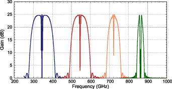
Figure 9 shows the simulated results, where we plot the gain-bandwidth product of our NbTiN device centered at 350 GHz, 550 GHz, 720 GHz and 860 GHz. As can be seen, for all four frequency bands, we managed to achieve a peak gain near 25 dB, indicating that it is potentially possible to operate a high-gap thin film KITWPA near its gap-frequency limit. At these frequencies, the design considerations are in some ways simpler as the inherent superconducting gap naturally supresses pump harmonics. However, one notices that the bandwidth of the device becomes progressively narrower at higher frequency bands. This is unsurprising given the nonlinear dispersion that becomes stronger at higher frequencies, as indicated in figure 3(b) before. It is possible to weaken the nonlinear dispersion at THz frequencies by engineering the thin film (e.g. using a thicker film) to reduce the high kinetic inductance to a certain degree while retaining the kinetic inductance required for amplification on the expanse of longer transmission line length. This solution, in principle, should not pose an issue at high-frequency operation since the physical length of the transmission line would be reduced substantially. Hence, it is possible to increase the total amplifier's electrical length substantially while maintaining the physical length within the fabrication limit.
Figure 9. Predicted gain profiles simulated for different operational frequency bands optimized to achieve peak gain of 25 dB.
Download figure:
Standard image High-resolution image
The last design in figure 9 poses an additional challenge due to the changing density of states near the gap from an applied pump current. Thorough modelling has shown that these effects become relevant at frequencies of 0.9Δ, meaning a substantially more robust model is required to accurately simulate the device operating above 800 GHz [28]. Although the more detailed analysis may show that this final device is not possible, it is presented here to demonstrate the rapid decrease in bandwidth as one approaches the superconducting gap. The remaining three designs fall sufficiently below the gap to largely avoid these effects and indicate the possibility of parametric amplification at high frequencies.
5. Conclusion
In this paper, we make use of the transmission profile of a fabricated Ka-band KITWPA device to recover the actual surface impedance of our NbTiN film; and to investigate the potential of applying the same technique to achieve a high parametric gain at mm/sub-mm wavelength. range. We found that by calibrating either the critical temperature or the normal resistivity of the film slightly and not taking into account the surface resistance, we can match the transmission profiles and the obtained gain-bandwidth product extremely well. We proceed to use this recovered thin film surface impedance to present a realistic design of a mm-wave KITWPA centered near 220 GHz, including the various design considerations for constructing a mm-wave KITWPA e.g. taking into account the effect of substrates, the design of the waveguide-to-planar circuit transformer, and the effect of the capacitive stubs that limits the bandwidth of these high-frequency TWPA. The proposed device has a bandwidth of about 130 GHz, which is wide enough to cover the entire ALMA Band-5 & 6 range. Finally, we extended our model to predict the upper-frequency limit of our device, showing that it is indeed possible to achieve high gain near the gap frequency of the film, albeit with a narrower bandwidth operation, which could be further remedied by engineering the kinetic inductance of the film to operate at mm/sub-mm wavelength.
Acknowledgments
This research was funded by the European Research Council (ERC) under the European Union's Horizon 2020 research and innovation programme with Grant Agreement No. [803862] (Project [SPA4AstroQIT]). For the purpose of Open Access, the author has applied a CC BY public copyright license to any Author Accepted Manuscript version arising from this submission. Dr Faramarzi's research was supported by appointment to the NASA Postdoctoral Program at the Jet Propulsion Laboratory, administered by Oak Ridge Associated Universities under contract with NASA. Any data that support the findings of this study are included within the article.
Data availability statement
All data that support the findings of this study are included within the article (and any supplementary files).