
Abstract
We investigate die-level and wafer-scale uniformity of Dolan-bridge and bridgeless Manhattan-style Josephson junctions, using multiple substrates with and without through-silicon vias (TSVs). Dolan junctions fabricated on planar substrates have the highest yield and lowest room-temperature conductance spread, equivalent to  in transmon frequency. In TSV-integrated substrates, Dolan junctions suffer most in both yield and disorder, making Manhattan junctions preferable. Manhattan junctions show pronounced conductance decrease from wafer center to edge, which we qualitatively capture using a geometric model of spatially-dependent resist shadowing during junction electrode evaporation. Analysis of actual junction overlap areas using scanning electron micrographs supports the model, and further points to a remnant spatial dependence possibly due to contact resistance.
Export citation and abstract BibTeX RIS

Original content from this work may be used under the terms of the Creative Commons Attribution 4.0 license. Any further distribution of this work must maintain attribution to the author(s) and the title of the work, journal citation and DOI.
1. Introduction
Monolithic superconducting quantum processors (SQPs) have scaled to enable key demonstrations of quantum-computational advantage [1] and milestone demonstrations of quantum error correction [2–4] on the road to fault-tolerant quantum computing. Sustaining this scaling requires a multi-faceted fabrication approach simultaneously meeting yield, frequency, coherence, and coupling requirements of circuit elements, as well as the routing of control lines needed for gate and measurement operations. The latter motivates the active development of 3D integration strategies such as flip-chip [5–7] to avoid overcrowding of circuit elements and vertical routing [8–10] of input and output lines to circumvent the scaling limitations associated with lateral wirebonding. Through-silicon visas (TSVs) are needed in some vertical routing approaches [11–14], and especially for suppression of resonance modes arising from the increased size of SQPs and their packaging.
TSVs further aggravate the targeting of superconducting qubit frequencies, which already bottlenecks the yield of operable devices even on planar substrates [15]. Poor qubit frequency targeting is a primary cause of crosstalk induced by microwave drives [2] and can limit gate speeds. It also increases residual ZZ coupling in processors with always-on qubit-qubit coupling [2, 3, 16], making gate fidelity and leakage dependent on the state of spectator qubits [17]. Laser annealing of qubit Josephson junctions (JJs) [15, 18–21] is an established method for selective qubit frequency trimming without intrinsic effect on qubit coherence. Currently, laser annealing allows a monotonic decrease with  range and
  imprecision (defined as the standard deviation of frequency targeting error post-annealing) [21]. To safely rely on laser annealing for post-fabrication trimming, fabrication itself must achieve an imprecision several times lower than the tuning range, e.g.
  .
.
The main limit to qubit frequency targeting is variability in the fabrication of  -
- -
- JJs, which most commonly relies on double-angle shadow evaporation with intermediate in-situ oxidation. Two main variables affecting the Josephson coupling energy
  are the overlap area between the two
  electrodes and the tunnel barrier thickness. The two most popular JJ fabrication variants differ only in the shadowing mechanism: Dolan-bridge [22] junctions use a suspended resist bridge whereas Manhattan-style [23] junctions do not. Since Dolan JJs are more sensitive to resist-height variation by design, Manhattan JJs may be preferable particularly on substrates with TSVs that compromise the uniformity of spin-coated resist. Previous works have shown a reduction in wafer-scale variation of Manhattan JJs [24, 25]. On the other hand, recent reports [26–28] indicate that geometric effects cause pronounced center-to-edge variation in Manhattan JJs, affecting their uniformity at wafer scale.
In this work, we present an experimental investigation comparing the uniformity of Dolan versus Manhattan JJs at both die- and wafer-scale on planar substrates with and without TSVs. We benchmark uniformity using room-temperature (RT) conductance (G) measurements, extracting the conductance coefficient of variation (CV) and residual standard deviation (RSD) of predicted transmon frequency. A wafer-center-to-edge variation is again observed particularly in Manhattan junctions, which we attribute to a geometric shadowing effect during electrode evaporation. Scanning electron microscopy (SEM) of many junctions supports the model, and further points to remnant spatial dependence possibly due to contact resistance. Our findings indicate that for our current fabrication processes, Dolan JJs perform best for planar substrates, while the opposite holds for TSV-integrated substrates. We identify several paths for further required improvement.
2. Design of experiments
We investigate uniformity of Dolan and Manhattan JJs using six 100  diameter
  wafers. (Sections S1 and S2 of the Supplementary Information provide detailed descriptions of the fabrication processes used.) Three of these wafers, labeled Planar 17Q (quantity one) and TSV 17Q (quantity two), are used to obtain and compare metrics for both junction variants in fully planar substrates and TSV-integrated ones. Each wafer contains thousands of test structures, each consisting of two nominally identical JJs connecting in parallel to pre-fabricated
  probing pads (
 thick, defined by sputtering and etching). These test structures mimic the two-junction transmon with
  capacitor plates used in our standard SQPs (figure 1(a)).
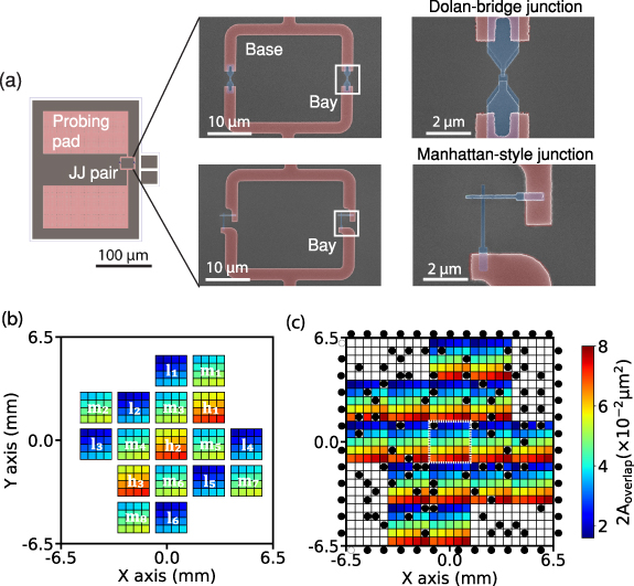
Figure 1. (a) Schematic and SEM images at two length scales of the test structures used to investigate uniformity of Dolan versus Manhattan JJ pairs on planar and TSV-integrated wafers. Two junctions in each structure complete a loop with a pre-fabricated  base. Probing pads in the base allow measuring the parallel conductance of the junction pair. (b) Die-level planar layout with 17,
  sub-arrays of junction test structures. Each array is centered at the location of one transmon in our planar Surface-17 SQP. Each array has a sweep of junction overlap area
  in one of three ranges (labeled l, m and h). (c) Die-level TSV layout arranged as 17,
  sub-arrays of junction test structures. Each array is centered at the location of one transmon in our TSV-integrated Surface-17. One such array is highlighted by the white dotted line. Each array has an identical sweep of
  . Test structures that overlap with vias (black circles) are ignored and not included in measurements, yielding at most 378 test structures per die. Heatmaps in (b) and (c) indicate the chosen
  for each test structure.
Download figure:
Standard image High-resolution imageIn the Planar 17Q wafer, a  mm die-level layout mimicking our planar 17-qubit SQP (Surface-17 [11, 21, 29]) is copy-pasted into two
  arrays. The top half of the wafer has test-structure arrays for Dolan-bridge JJs, while the bottom half has test-structure arrays for Manhattan-style JJs. At the location of each transmon of the SQP, we place a sub-array of
  test structures. Within each sub-array (figure 1(b)), the designed single-junction overlap area (
 ) is finely stepped within one of three ranges, labeled low (l), mid (m) and high (h), mimicking the choice of three qubit-frequency groups in our SQPs [11, 16, 21, 29]. For Dolan-bridge JJs, we change
  by varying the width
  of the top electrode and keeping the width of the bottom electrode
  . For Manhattan-style JJs, we instead vary
  and fix
  . In total, the wafer contains 2176 test structures of each JJ variant. We first fabricate only the Manhattan JJs on the bottom half of the wafer and perform all conductance measurements on them. We subsequently fabricate and measure all Dolan JJs on the top half of the wafer. Each TSV 17Q wafer contains test structures of only one JJ variant. In each wafer, the die-level layout (copy-pasted into one
  array) has TSVs placed at the same locations as a variant of Surface-17 with TSVs (figure 1(b)). The density (
 area coverage) and position of TSVs is chosen to push the lowest-frequency spurious modes of the SQP in its sample holder to
  (as per finite-element simulation). At the location of each transmon in the SQP, we place a
  sub-array of test structures. In this case, all sub-arrays are identical. Importantly, test structures overlapping with TSVs, although fabricated, are ignored and not included in conductance measurements. This yields at most 378 viable test structures per die and thus 3024 per wafer.
Three additional wafers, labeled Planar  , are used to test the geometric resist-shadowing model and to investigate further sources of spatial non-uniformity in Manhattan JJs. Each wafer (figure 5) has a
  array of nominally identical test structures
  . In the first wafer, like in the 17Q wafers, the test structures have symmetric JJ pairs with
  probing pads. In the second, they have symmetric JJ pairs with
  probing pads (
 thick, pre-defined by atomic layer deposition (ALD) and etching). In the third, they have single JJs with
  probing pads evaporated simultaneously with the JJ electrodes.
3. Measurements and analysis
All G measurements are acquired by the 2-point method using a home-built transimpedance amplifier with gain  . A low input voltage
  is applied across the junctions to minimize the possibility of causing failure to open or short circuit. With one exception noted below, measurements on all planar wafers are performed using a manual probe station located inside our cleanroom, which is temperature controlled to
  . During manual measurements, the intensity from a light-emitting diode source is set to the lowest possible visibility
  , limiting the contribution from substrate conductance to
  , as determined from G measurements on test structures both without JJs and with JJs known to have failed to open circuit. Measurements on the TSV 17Q wafers as well as on the Planar
  wafer are performed using a home-built automated probe station, also located inside the cleanroom, whose measurements are performed fully in the dark. To quantify series resistance from the probe contact and external cabling, we compared 2- and 4-point G measurements taken with the automated probe station, finding a best-fit value of
  . The series resistance of
  probing pads is found to vary from
  at wafer center to
  at wafer edge by fabricating test structures with bays short-circuited directly in the base layer. This variation is attributed to the radial dependence of the thickness of the sputtered
  films (resistivity
  ). Reported G values are raw, i.e. as obtained from 2-point measurement without correction for series resistance, substrate conductance, nor a
  offset from the transimpedance amplifier.
The range of G is  . Values
  and
and  are filtered out as they mostly correspond to open and shorted junctions, respectively. To systematically detect and filter out data containing an open junction in a pair, a two-part linear regression analysis of conductance versus
  is implemented within each die in the Planar and TSV 17Q wafers. Values below
  of the initial best fit are filtered out (figures S3 and S4). For the Planar
  wafers containing nominally identical test structures throughout, conductance values below
  of the mean are filtered out.
To quantify non-uniformity at both die and wafer scale, we use the conductance CV as a function of  and the RSD of predicted qubit frequency. Die-(wafer-) level conductance CV is calculated using all the test structures with identical
  across the die (wafer) when calculating the mean µG
and standard deviation σG
. The spatial variation of junction conductance is visualized using heatmaps of conductance normalized by µG
of all test structures with identical
across the die (wafer) when calculating the mean µG
and standard deviation σG
. The spatial variation of junction conductance is visualized using heatmaps of conductance normalized by µG
of all test structures with identical  . The predicted transmon qubit transition frequency
  is calculated from G using
where  with
with  the designed transmon charging energy,
  , and
, and  [30–32]. Here,
  is an experimentally determined constant obtained by comparing G measured immediately prior to cooldown to the
  extracted for transmons across many of our SQPs. (
 is extracted from spectroscopy data obtained during cryogenic characterization.) Die-level frequency RSD is calculated from the residuals of the second fit. Wafer-level RSD is calculated similarly, but the residuals are obtained by performing a single fit on the combined filtered G data from all dies.
To test the geometric resist-shadowing model, SEM images of JJs from different coordinates on all Planar  wafers are acquired at
  magnification. A total of 34 (35) JJ pairs are imaged for the
  (
( ) wafer, and 36 single JJs for the
  wafer. Imaging is performed only after conductance measurements are completed. The actual deposited junction widths (
 ,
,  ) and overlap area
  are extracted using home-made image analysis software (based on the OpenCV package) with the work flow presented in figure S8. The presence of other sources of spatial non-uniformity is evidenced from the spatial dependence of effective JJ conductivity calculated as
  .
.
4. Results
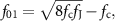
A total of 2176 (3024) test structures are fabricated per JJ variant for the Planar and TSV 17Q datasets. A zoomed-out view (figure 2) of the planar dataset shows that the spatial variation of normalized conductance for Dolan JJs is significantly lower than for Manhattan JJs. For the latter, there is a clear systematic decrease from center to edge, making it unsurprising that the wafer-scale conductance CV is higher for Manhattan over all  . The general decrease observed in the conductance CV with increasing
  is in line with previous works [33, 34]. At die level, the spread of Dolan JJs is also lowest, with
  frequency RSD uniform across the wafer. For Manhattan JJs, the frequency RSD increases away from wafer center, indicating that the spatial variation is relevant even at die level.
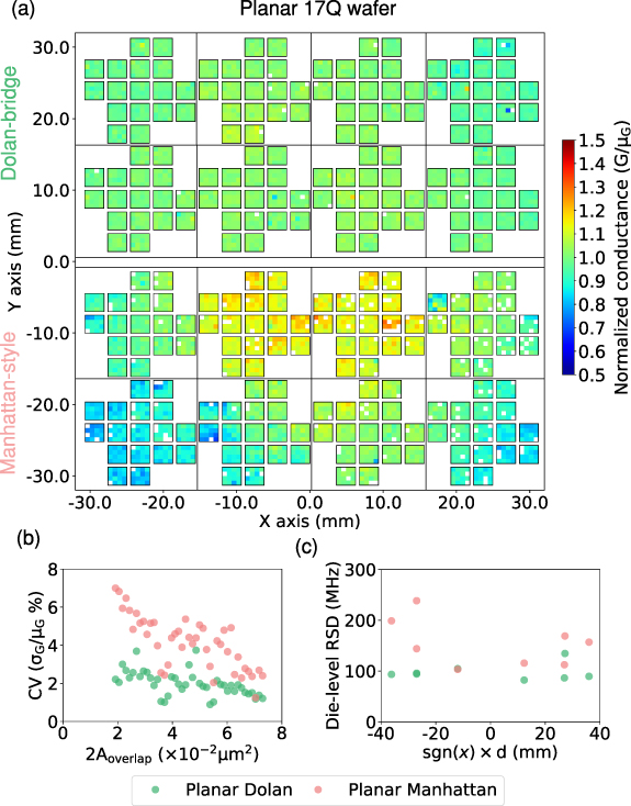
Figure 2. (a) Wafer-scale mean-normalized conductance heatmap of Dolan (top) and Manhattan (bottom) JJ test structures on the Planar 17Q wafer. The origin  indicates wafer center. Blank cells correspond to test structures identified as defective by the filtering. For this dataset, both JJ types are fabricated on a single wafer. (b) Wafer-scale conductance CV for both junction types as a function of
  . (c) Die-level RSD of predicted qubit frequency as a function of distance (d) between die and wafer centers.
Download figure:
Standard image High-resolution imageTurning over to the TSV dataset (figure 3), we can again discern an underlying center-to-edge dependence for Manhattan JJs. However, this trend is masked by a significant increase in disorder. The disorder is much stronger for Dolan JJs, evident both at wafer scale and die level. Interestingly, the CV for Dolan does not display any clear dependence on  , suggesting that resist-height variations dominate the spread. Measurements of resist-height variations caused by TSVs and evidence of the impact of such variations on junction electrode and overlap geometries are shown in figure S2.

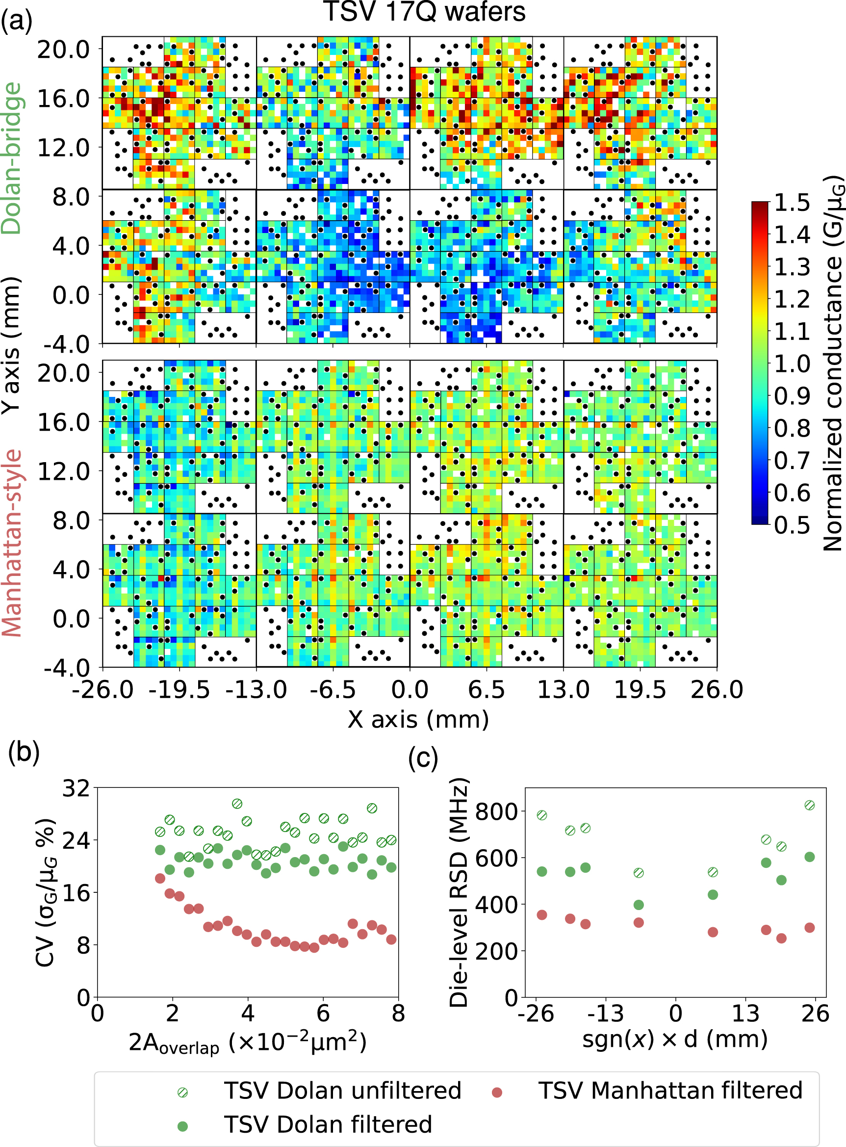
Figure 3. (a) Wafer-scale mean-normalized conductance heatmap of Dolan (top) and Manhattan (bottom) JJ test structures on TSV-integrated 17Q wafers. For this dataset, two separate wafers are fabricated, one for each JJ type. The origin  indicates wafer center. Blank cells correspond to defective junctions removed by filtering outliers at die level. Cells marked with black circles indicate TSV locations. (b) Wafer-scale conductance CV for unfiltered (nf) and regression-filtered (f) Dolan JJ pairs and for filtered Manhattan JJ pairs as a function of
  . (c) Die-level RSD of predicted qubit frequency as a function of distance (d) between die and wafer centers.
Download figure:
Standard image High-resolution imageNote that the CV and RSD for Dolan are calculated both with and without applying regression filters. This is necessary because the high disorder makes the regression filter unable to reject only defective junctions. Even with the artificial improvement of Dolan CV and RSD that may arise from removing non-defective junctions, a strong conclusion holds: with TSVs, Manhattan JJs systematically outperform Dolan JJs. Nonetheless, with  RSD at die level, even Manhattan JJs fall very short of frequency targeting objectives in the presence of TSVs. However, there is room for optimism as this investigation is best interpreted as a worst-case scenario for actual TSV-integrated SQPs. In our test, we place many junction pairs per transmon location of Surface-17. Therefore, in a real Surface-17, transmon JJ pairs would on average be
  away from TSVs. Furthermore, the footprint of TSVs could be further optimized following [12].
4.1. Geometric resist-shadowing model
The essence of the geometric model is a spatial dependence of junction electrode widths arising from oblique incidence of the  flux during evaporation. Specifically, the width of vertical electrodes (both electrodes for Dolan JJs, bottom electrode for Manhattan JJs) depends on the x coordinate, while that of horizontal electrodes (top electrode for Manhattan) depends on the y coordinate. Key parameters of the model are the thickness of the top resist
  (which acts as the shadow mask), the wafer tilt
  during
  evaporations, and the physical configuration of the electron-beam (e-beam) evaporator (Plassys MEB550S). These last parameters include the distance
  between the crucible at
  and the pivot point
  of the sample holder, and the distance
  between
  and center
  of the exposed wafer surface (see schematic in figure 4(a)). This results in a distance
  between
  and the plane defined by this surface [35]. In a cartesian coordinate system with origin at
  and
and  lying on this plane,
  . Evaporation under these conditions deposits electrodes extending along the y axis. An electrode of this orientation with x coordinate has actual width

where  is a constant widening from over-exposure and development of the e-beam resist. Including these modifications to the width of both electrodes, the actual overlap area becomes

Figure 4(b) shows the spatial dependence of  for Manhattan JJs with
  and
and  on a 100-
 diameter wafer.
Figure 4. (a) Schematic of e-beam  evaporation setup (not drawn to scale). Please see text for further details and parameter values. The illustration shows the decrease in junction electrode width from center to edge of wafer arising from the spatially-dependent shadowing effect. (b) Wafer-scale mean-normalized conductance computed from actual junction overlap area
  as per equation (2), for Manhattan JJs with
  and
and  . (c) Same as (b) but adding the overlap contribution from sidewalls as per equation (4). (d) Same as (c) but adding effects of the first evaporation (of the bottom electrode) on the second evaporation (of the top electrode) (equations (5)–(7)).
Download figure:
Standard image High-resolution imageWe can further expand the model by approximating the contribution of sidewalls to  . The spatially-dependent actual bottom electrode thickness is
where  is the calibrated thickness at
  under normal incidence
  . Approximating the sidewalls as vertical,

The modified spatial dependence is shown in figure 4(c). Note that we do not model the effect of shadowing by the bottom electrode during evaporation of the top electrode, which most likely reduces the overlap at the eastern sidewall (evident in figure S9).
Finally, we can model some predictable effects of the first evaporation (for the bottom electrode) on the top electrode. The first evaporation deposits an  layer above the top resist, effectively increasing its height by
  (also given by the right-hand side of equation (3)). More importantly, it also deposits a lip on the southern resist edge for the top electrode (see figure S1), with width
  and height
  :
:


The shadowing effect of these features makes

where  and
and  . Including all modeled effects leads to
  as shown in figure 4(d).
The geometric model predicts that junction conductivity erroneously computed as  will show a center-to-edge decrease. Experimental results for the three Planar
  wafers clearly show this trend (figures 5(g)–(i)). In turn, the model predicts that conductivity computed as
  will be flat. Due to the inaccuracy of approximating
  using top-view SEM images, a slight center-to-edge increase could even be observed. Conductivity computed as
  is very uniform for the all-
 wafer, but not for the wafers with
  and
and  probing pads. In these, the conductivity is very similar (
 ) at wafer center, but decreases noticeably away from it. These observations suggest that series resistance from the contact region (nominally
  ) between
  electrodes and the
  or
or  bays is small at wafer center but increases significantly away from center. While the contact region area is also impacted by the geometric shadowing effect, fractionally the effect is much less significant than for the JJ overlap areas, and cannot explain the observation. Using circuit analysis, we can calculate the net contact series resistance per junction required to match the observed reduction in conductivity computed from
  at wafer edge. We find
  for
for  pads and
  for
for  pads.
pads.

Figure 5. Wafer-scale mean-normalized conductance heatmap of  array of Manhattan JJ test structures fabricated on three planar wafers with the variants indicated by the top schematics. (a), (b) Symmetric junction pairs with (a)
  probing pads deposited by sputtering and (b) TiN probing pads deposited by ALD. The black dotted line indicates the diagonal along which the JJ pairs are imaged for figure S9. (c) Single junctions with simultaneously fabricated
  probing pads. The hatched rows indicate accidentally omitted junctions during data acquisition. (d)–(f) Distribution of actual JJ overlap area
  as a function of junction radial position (d). Here,
  is extracted from top-view SEM images. Note that
  does not include the sidewall overlap as this contribution cannot be extracted from these images. The black curves are the best fits of the simplest geometric model (equation (2) with single free parameter
  ). (g)–(i) Effective junction conductivity (computed from designed and actual overlap areas) as a function of d. The dashed (solid) curves are quadratic fits of
  (
( ).
).
Download figure:
Standard image High-resolution image
It remains important for future research to directly measure the magnitude and spatial dependence of this contact resistance, and to reduce both using bandaging layers [33, 36].
5. Conclusions
Table 1 summarizes the findings of our investigation of Dolan and Manhattan JJs on planar and TSV-integrated substrates, spanning yield, conductance CV and frequency RSD at wafer level, as well as average die-level RSD. For planar substrates, Dolan JJs perform best in all categories. In TSV-integrated substrates, Dolan JJs show a marked increase in disorder and decrease in yield, most likely due to their higher susceptibility to resist-height variation. Manhattan JJs are thus the preferred choice for TSV-integrated substrates, but their uniformity must be further improved. First, we must pre-compensate the spatial variation of junction overlap area that arises from the shadowing effect captured by the geometric model. For the Manhattan-JJ resist stack used, the model predicts a narrowing of electrode widths by  from wafer center to edge (see figure S7). The resolution of our e-beam lithography system in
  write mode is
  , and thus it is possible in principle to pre-compensate the spatial variation in
  . Next, the magnitude and strong spatial dependence of contact resistance between the
  electrodes and the
  bays, only inferred from our data, should be quantified, understood, and hopefully diminished using bandaging layers. These improvements will allow to quantify the intrinsic disorder of Manhattan JJs and approach the
  target that will secure SQP yield by post-fabrication trimming using laser annealing.
Table 1. Summary of metrics obtained for Dolan and Manhattan JJ test structures on all wafers used throughout this study. The 17Q yield reported is that calculated for a Surface-17 SQP using the per-junction-pair yield of the Planar and TSV 17Q wafers. We note that the yield of actual planar Surface-17 SQPs with Manhattan-style JJs is roughly  , higher than that calculated from the Planar 17Q wafer. The die-level frequency RSD is the average across the eight dies in the 17Q wafers. For the
  Planar wafers, the die-level frequency RSD is calculated from the average of sixteen
  arrays of test structures within the inner
  area of the wafers.
| Summary of results | |||||
|---|---|---|---|---|---|
| Conductance | Frequency | Frequency | |||
| CV wafer | RSD wafer | RSD die | |||
| Junction type | Substrate | Yield (%) | scale (%) | scale (MHz) | level (MHz) |
| Dolan-bridge | Planar 17Q NbTiN | 2160/2176 = 99.2 | 0.8–3.7 | 140 | 98 |
| 17Q yield = 87.2 | |||||
| TSV 17Q NbTiN | 2958/3024 = 97.8 | 21.6-29.5 | 800 | 681 | |
17Q yield = 68.5
| |||||
| 2770/3024 = 91.6 | 18.5-22.5 | 666 | 520 | ||
17Q yield = 22.5
| |||||
| Manhattan-style | Planar 17Q NbTiN | 2006/2176 = 92.2 | 1.2–7 | 317 | 155 |
| 17Q yield = 25.1 | |||||
| TSV 17Q NbTiN | 2867/3024 = 94.8 | 7.5–18 | 342 | 306 | |
| 17Q yield = 40.3 | |||||
Planar  NbTiN NbTiN | 1176/1225 = 96.0 | 11.3 | 549 | 182 | |
Planar  TiN TiN | 1161/1225 = 94.8 | 8.9 | 446 | 172 | |
Planar  Al Al | 1121/1155 = 97.0 | 6.8 | 251 | 119 | |
a Without regression filtering. b With regression filtering. c Two rows were accidentally omitted during data acquisition.
Acknowledgments
We thank Bas van Asten for experimental assistance and David Michalak for valuable discussions. This research is supported by Intel Corporation and by the Office of the Director of National Intelligence (ODNI), Intelligence Advanced Research Projects Activity (IARPA), via the U.S. Army Research Office Grant No. W911NF-16-1-0071. The views and conclusions contained herein are those of the authors and should not be interpreted as necessarily representing the official policies or endorsements, either expressed or implied, of the ODNI, IARPA, or the U.S. Government.
Data availability statement
The data that support the findings of this study are openly available at the following URL/DOI: http://github.com/DiCarloLab-Delft/Wafer_Scale_Fab_Data.
Additional information
The data shown in all figures of the main text and Supplementary Information are available at http://github.com/DiCarloLab-Delft/Wafer_Scale_Fab_Data. Correspondence and requests for additional materials should be addressed to L.D.C. (l.dicarlo@tudelft.nl).
Supplementary data (13. MB PDF)