
Abstract
Ruthenium dioxide (RuO2) is a metallic rutile oxide with a number of interesting properties. For a long time, it was considered to be a highly conductive normal metal and a Pauli paramagnet. Recently, it was found that the material is antiferromagnetic, with small magnetic moments of the order of 0.05 Bohr magneton and an ordering temperature above 300 K. The presence of magnetic moments should have clear consequences when trying to induce superconductivity in RuO2. We used a selective area chemical vapor deposition method to grow nanostrips of RuO2 on TiO2 substrates. On these nanostrips, superconducting contacts were made of MoGe, and a weak link was fabricated with a Focused Ion Beam. We find that the device behaves as a Josephson junction, including a Fraunhofer-like response to a magnetic field, for distances between the contacts below 70 nm. We estimate the induced singlet coherence length ξ to be about 12 nm, which seems a reasonable number when small magnetic moments are present.
Export citation and abstract BibTeX RIS

Original content from this work may be used under the terms of the Creative Commons Attribution 4.0 license. Any further distribution of this work must maintain attribution to the author(s) and the title of the work, journal citation and DOI.
1. Introduction
In recent years, there has been a revival of interest in the properties of the metallic rutile oxides CrO2, RuO2 and IrO2, mainly in connection with magnetism, non-trivial Fermi surfaces, and possible spintronics applications [1, 2]. CrO2 is a half-metallic ferromagnet that in bulk form was long used in magnetic tapes [3] and in thin film form was found of particular interest to study superconducting long rang range proximity effects [4–6]. IrO2 was researched from a spintronics perspective as a material with large spin–orbit coupling [7, 8]. RuO2 was long thought to be a normal metal, and in film form often used in low-temperature thermometry, because of ease of use and insensitivity of the resistance to even high magnetic fields. However, in 2017 itinerant antiferromagnetism was discovered [9], with magnetic moments of the order of 0.05 µB (with µB the Bohr magneton) and a (Néel) ordering temperature above 300 K. This was confirmed in another study [10], and also prompted renewed studies of the anomalous Hall effect [11, 12]. On the other hand, also superconductivity was recently reported in slightly strained films of RuO2 [13].
Long range proximity effect has been recently observed in Mn3Ge, resulting from the chiral non-collinear antiferromagnetic spin structure that creates a non-zero Berry phase [14]. The same study also reported that IrMn, a collinear antiferromagnet with moments on the Mn site of the order of 3 µB (Bohr magneton) [15], only shows short range supercurrents owing to its trivial topological spin arrangement. RuO2, although also a collinear antiferromagnet, has been shown to have crystal inversion asymmetry arising from spin-splitting and time-reversal symmetry breaking in the band structure [16–18]. RuO2 has also been identified as a promising candidate to allow for spin polarized currents which has been substantiated by recent transport measurements conducted on RuO2 [19–21]. In this work, we investigate the proximity effect in RuO2 nanostrips by fabricating lateral Josephson junctions, using superconducting amorphous MoGe as electrodes. Since the resistivity of RuO2 is quite low, we can expect a quite long induced coherence length if the material behaves as a normal metal. Instead, and confirming the presence of (small) magnetic moments, we find a short decay length (ξ) of around 12 nm which indicates the presence of only short range singlet Cooper pairs and absence of long range spin triplets. The paper is organized in the following manner. We begin by examining the nanofabrication process that leads to Selective Area (SA)-grown nanostrips. Subsequently, we proceed to characterize these RuO2 nanostrips through electrical and magneto-transport measurements. Then we focus on making Josephson junctions (JJ) in which superconducting MoGe are contacted on top of RuO2 nanostrips with varying lateral gaps and present the results on these junctions.
2. Selective area growth of RuO2 nanostrips
We grow RuO2 nanostrips on (100) oriented TiO2 substrates using the same selective area growth technique as CrO2 nanostrips [22] since the lattice parameters of TiO2, RuO2 and CrO2 are comparable and they all crystallize with a rutile structure and a tetragonal unit cell. RuO2 has the attice parameters a = b = 0.4499 nm and c = 0.3107 nm while TiO2 has the values of a = b = 0.4594 nm and c = 0.2958 nm. Compared to the TiO2 lattice, the [010] and [001] directions of bulk RuO2 have a lattice mismatch of approximately −2.1% and +5.0% respectively. Thus, RuO2 thin films experience tensile strain along [010] while compressive strain along [001].
The fabrication of the RuO2 nanostrip starts with an HF etch of TiO2 substrate. This is then followed by depositing a SiOx
layer, which in our case has a thickness of approximately  nm, and electron beam patterning to create a positive resist mask with the desired device structure. Subsequently, the trench is selectively etched using reactive ion etching (RIE). We have observed that both underetching and overetching the trench is detrimental for a successful growth, similar to the case of CrO2. RuO2 nanostrips are subsequently grown in the trenches using chemical vapor deposition (CVD) in a two-zone furnace. During this process, the substrate temperature is maintained at 390 °C while the precursor (C5H5)2 Ru is heated to 80 °C in the presence of an O2 carrier gas flow. Figure 1(a) shows the SEM image of an epitaxially grown RuO2 nanostrip along the [001] direction. RuO2 also grows on the surface of SiOx
[23] albeit much more slowly than on TiO2 which helps to prevent merging of small crystals of RuO2 of a few tens of nanometers in diameter that also form during nanostrip growth.
nm, and electron beam patterning to create a positive resist mask with the desired device structure. Subsequently, the trench is selectively etched using reactive ion etching (RIE). We have observed that both underetching and overetching the trench is detrimental for a successful growth, similar to the case of CrO2. RuO2 nanostrips are subsequently grown in the trenches using chemical vapor deposition (CVD) in a two-zone furnace. During this process, the substrate temperature is maintained at 390 °C while the precursor (C5H5)2 Ru is heated to 80 °C in the presence of an O2 carrier gas flow. Figure 1(a) shows the SEM image of an epitaxially grown RuO2 nanostrip along the [001] direction. RuO2 also grows on the surface of SiOx
[23] albeit much more slowly than on TiO2 which helps to prevent merging of small crystals of RuO2 of a few tens of nanometers in diameter that also form during nanostrip growth.

Figure 1. (a) SEM image (false color) of a RuO2 nanostrip grown using Selective Area Growth. The magnetic field B is applied out of the plane for Hall characterization measurements. (b) Longitudinal resistivity as a function of temperature for a RuO2 nanostrip with dimensions of approximately  m in length between contacts and
  nm in width; inset shows the positive temperature coefficient of resistance at lower temperature indicating that high crystal quality. (c) mobility (µe
) (top) and charge carrier density (ne
) (bottom) at different temperature indicating that the behavior is unlike normal metal where ne
stays constant with temperature (d) Hall resistivity as a function of applied field measured at various temperature between
nm in width; inset shows the positive temperature coefficient of resistance at lower temperature indicating that high crystal quality. (c) mobility (µe
) (top) and charge carrier density (ne
) (bottom) at different temperature indicating that the behavior is unlike normal metal where ne
stays constant with temperature (d) Hall resistivity as a function of applied field measured at various temperature between  K to
K to  K.
K.
Download figure:
Standard image High-resolution imageFigure 1(b) shows the temperature dependence of the resistivity, ρxx
(T) of a typical RuO2 nanostrip, that was patterned as a Hall Bar of width around 650 nm, thickness around 100 nm and with a distance between the contacts around  m. The 300 K resistivity ρ300 is
  .cm while the low-temperature (10 K) specific resistance ρ10 is
  .cm. This gives a residual-resistivity ratio (RRR, the ratio between ρ300 and ρ10) of around 5.3. The nanostrip has a positive temperature coefficient of resistance at all temperatures including at low temperatures, as seen in inset of figure 1(b), which suggests very little or no grain boundary scattering of electron and a high crystal quality of the RuO2 nanostrips.
We further characterized RuO2 nanostrip through Hall measurements at different temperatures. Figure 1(d) shows measurements of the Hall resistivity as a function of an out-of-plane magnetic field for different temperatures in a range from 300 K to 10 K. The data are represented as ρxy
as function of magnetic field, with  . Here, V
 is the transverse voltage, I is the measurement current, and t is the thickness of the nanostrip.
  is linear for all the measured temperatures and the field with a slope that corresponds to electron-like charge carriers. Carrier density (n) and mobility (µe
) follow in a one-band model from
is linear for all the measured temperatures and the field with a slope that corresponds to electron-like charge carriers. Carrier density (n) and mobility (µe
) follow in a one-band model from  and
and  where, σxx
is
where, σxx
is  . Their values and temperature dependence are plotted in figure 1(c). It is interesting to note that charge carrier density decreases with temperature and is nearly 4 times lower at 10 K than at 300 K.
3. Methods
Junction fabrication: To fabricate the lateral JJs (figure 2(a)), the initial step involved using SA technique to grow RuO2 nanostrips with dimensions of approximately  m in length and
  nm in width, along the [001] direction. Superconducting contacts were fabricated by a combination of e-beam lithography and focused ion beam (FIB) milling (FIB). First, a liftoff resist structure was prepared, with a trench of about 2 micron wide, perpendicular to the nanostrip. Then,
  nm of MoGe was sputter deposited at a pressure of
  mbar, leading to the contact strip after lift-off. Finally, the weak link was created using FIB etching using a 10 keV Ga ion beam with a beam current of 15 pA. This way of preparing junctions is similar to earlier work we performed on various disk structures [24, 25]. In this way, three different junction devices were fabricated, with an edge-to-edge gap between the MoGe contacts of 32 nm (J1), 61 nm (J2) and 105 nm (J3). Here, a caveat is needed. In particular the 32 nm trench is both hard to make uniform, and proved not easy to measure in the SEM. The estimate should rather be 27 nm–38 nm. Moreover, the cut for this sample also made the nanostrip locally smaller. For the wider bridges, fewer issues were experienced. Also, generally, the cuts were quite deep, meaning that the RuO2 bridge was thinner than its nominal value. Still, some clear conclusions can be drawn, as we will discuss below. Figures 2(a) and (b) shows the SEM images (false color) of the devices J1 and J2 respectively, consisting of RuO2 nanostrip (blue) and MoGe electrodes (peach) on top of RuO2. Figures 2(c) and (d) give their corresponding resistive transitions. The critical temperature of the MoGe is about 7 K, and visible as a tiny step (in J1), or a deviation from constant resistance (J2). A clear drop in resistance due to the contacts going superconducting is not expected, since this is a 4-point measurement. The normal state resistance in both cases (about 3 Ω for J1, 0.8 Ω for J2) is quite different, mainly due to the difference in trench depth. The transition temperature Tc
, defined by the midpoint of the resistive transition, was also different, about 5.5 K for J1, and about 4 K for J2. These devices, with the smallest gaps, showed clear Josephson junction behavior. Device J3 with a 105 nm gap proximized only partially, meaning that zero resistance was not reached till 1.5 K. Table 1 summarizes the basic device parameters.
mbar, leading to the contact strip after lift-off. Finally, the weak link was created using FIB etching using a 10 keV Ga ion beam with a beam current of 15 pA. This way of preparing junctions is similar to earlier work we performed on various disk structures [24, 25]. In this way, three different junction devices were fabricated, with an edge-to-edge gap between the MoGe contacts of 32 nm (J1), 61 nm (J2) and 105 nm (J3). Here, a caveat is needed. In particular the 32 nm trench is both hard to make uniform, and proved not easy to measure in the SEM. The estimate should rather be 27 nm–38 nm. Moreover, the cut for this sample also made the nanostrip locally smaller. For the wider bridges, fewer issues were experienced. Also, generally, the cuts were quite deep, meaning that the RuO2 bridge was thinner than its nominal value. Still, some clear conclusions can be drawn, as we will discuss below. Figures 2(a) and (b) shows the SEM images (false color) of the devices J1 and J2 respectively, consisting of RuO2 nanostrip (blue) and MoGe electrodes (peach) on top of RuO2. Figures 2(c) and (d) give their corresponding resistive transitions. The critical temperature of the MoGe is about 7 K, and visible as a tiny step (in J1), or a deviation from constant resistance (J2). A clear drop in resistance due to the contacts going superconducting is not expected, since this is a 4-point measurement. The normal state resistance in both cases (about 3 Ω for J1, 0.8 Ω for J2) is quite different, mainly due to the difference in trench depth. The transition temperature Tc
, defined by the midpoint of the resistive transition, was also different, about 5.5 K for J1, and about 4 K for J2. These devices, with the smallest gaps, showed clear Josephson junction behavior. Device J3 with a 105 nm gap proximized only partially, meaning that zero resistance was not reached till 1.5 K. Table 1 summarizes the basic device parameters.

Figure 2. SEM image (false color) of the fabricated Josephson junctions (JJ) comprising RuO2 nanostrip (in blue) and MoGe as the superconducting contacts (in peach) that are laterally edge to edge separated by (a) 32 nm for J1 and (b) and 61 nm for J2. (c), (d) Resistance vs temperature plot between (10–1.5) K showing the transition temperature (Tc
) for the junctions (c) J1 and (d) J2. We have taken Tc
as the temperature at which the resistance has decreased to  of the normal resistance value, which for J1 is 5.5 K and for J2 is 3.8 K.
Download figure:
Standard image High-resolution imageTable 1. Critical current at measured temperature, normal resistance, junction length and the corresponding critical voltage of three Josephson junction devices based on nominally 100 nm thick and 250 nm wide RuO2 nanostrips, contacted with 100 nm thick superconducting MoGe.
| Device | T (K) |
 ) ) |

|

|

|
|---|---|---|---|---|---|
| J1 (E5−2.1) | 1.8 | 121 | 2.85 | 32 ±6 | 345 |
| J2 (H4−1.1) | 1.8 | 33 | 0.86 | 61 | 28.3 |
| J3 (E5−1.2) | 1.5 | 0 | 3.11 | 105 | 0 |
4. Results and discussion
We measured the zero-field current(I)–voltage(V) behavior of the two JJs J1 and J2 as function of temperature. Typical IV characteristics are shown in figures 3(a) and (b) while figures 3(c) and (d) shows the color plot of I versus the derivative-dV/dI. We extracted the  from the onset of a change in the derivative, shown by the dashed line (white) in the figures 3(c) and (d). With this criterion, the temperature of the onset of supercurrent roughly coincides with the temperature of the midpoint of the resistive transition. At the lowest temperatures, Ic
has become nearly constant. These low-temperature values show a strong decrease of Ic
with increasing gap, dropping from 121 µA in J1 to 33 µA in J2.
from the onset of a change in the derivative, shown by the dashed line (white) in the figures 3(c) and (d). With this criterion, the temperature of the onset of supercurrent roughly coincides with the temperature of the midpoint of the resistive transition. At the lowest temperatures, Ic
has become nearly constant. These low-temperature values show a strong decrease of Ic
with increasing gap, dropping from 121 µA in J1 to 33 µA in J2.

Figure 3. Current (I) versus Voltage (V) measurements taken above (black) and below (red) the superconducting transition of (a) J1 and (b) J2, respectively. Panels (c), (d) show the behavior of dV/dI as function of I, measured over different temperatures in steps of (c) 200 mK, for J1, and (d) 100 mK, for J2. The dashed white lines show the associated critical current Ic (T), extracted from a differential resistance criterion (0.4 Ω for (c), 0.6 Ω for (d)). Panels (e), (f) show that same Ic (T) (dashed blue line) together with Ic (T) derived from an Ambegaokar-Halperin fit to the I-V characteristics for (e) junction J1 and (f) junction J2.
Download figure:
Standard image High-resolution imageWe also employed a different way of extracting Ic
, by fitting the I-V characteristics to an analytical expression, derived from the work of Ambegaokar and Halperin [26]. More details on the fit can be found in the
We further fabricated and measured device J3 with a gap ds
= 105 nm, which did not reach zero resistance. Figure 4(a) shows the R(T) measurement from 300 K down to 1.5 K. We observe that the resistance becomes constant below 10 K, with a value of  around 8 K. When the MoGe electrodes become superconducting at 6.8 K the resistance starts to decrease again (after a small dip-peak excursion) but does not reach
  . The dip-peak feature hints at a slightly inhomogeneous superconducting transition [27] This behavior suggests that the RuO2 nanostrip did not proximize completely over the whole length of the junction. In contrast, a reduction of around 41% in resistance from the normal state resistance is seen when the temperature is lowered to 1.5 K. This reduction translates to a proximity length of about 20 nm extending from each contact.

Figure 4. (a) SEM image of the device J3 where  nm. (b) I-V characteristics measured at 2.5 K (black) and 1.5 K (red) at zero-field shows very small non-linearity. The inset shows a zoom-in of the non-linear behavior starting to occur at 1.5 K (red). (c) R(T) behavior of J3 measured from 280 K down to 1.5 K. The inset shows the R-T for temperature between 9 K to 1.5 K. A sharp drop in resistance is measured around 6.8 K signaling the superconducting transition MoGe. By 1.5 K, the normal state resistance of the strip has dropped by 41% which is a clear signature of partial proximization of the junction. (d)
  as a function of ds
for the 3 JJ devices. The red curve is the fitted exponential decay function which gives coherence length (ξ) in RuO2 of around 12 nm.
as a function of ds
for the 3 JJ devices. The red curve is the fitted exponential decay function which gives coherence length (ξ) in RuO2 of around 12 nm.
Download figure:
Standard image High-resolution imageUsing the three JJ devices parameters, the coherence length ξ of the supercurrents can be estimated. For this, we use the decay of the coupling strength, given by the product  . This ensures that the actual dimensions of the bridge, as given by RN
, are taken into account correctly. We fit
. This ensures that the actual dimensions of the bridge, as given by RN
, are taken into account correctly. We fit  using an exponential decay function
  . There are only three data points,but the fit does show compatibility with exponential behavior. For our devices we estimate ξ ≈ 12 nm as shown in the figure 4(d). This matches quite well with the proximity length that we estimated to be induced in the longer junction J3. We also note that the order of magnitude reflects the size of the Ru-moment: in the collinear AF magnet IrMn, with a Mn moment of 3 µB
, the coherence length was estimated 3–5 nm [14] (even quite large for such moments, possibly because it is an AF); in weak ferromagnets such as Pd
. There are only three data points,but the fit does show compatibility with exponential behavior. For our devices we estimate ξ ≈ 12 nm as shown in the figure 4(d). This matches quite well with the proximity length that we estimated to be induced in the longer junction J3. We also note that the order of magnitude reflects the size of the Ru-moment: in the collinear AF magnet IrMn, with a Mn moment of 3 µB
, the coherence length was estimated 3–5 nm [14] (even quite large for such moments, possibly because it is an AF); in weak ferromagnets such as Pd Nix
or Cu
Nix
or Cu Nix
, it is found that the superconducting decay length (the dirty-limit coherence length ξF
) is of the order of 5 nm for magnetic moments in the range 0.1–0.2 µB
[28–30]. Finding 12 nm for an AF with moments of 0.05 µB
appears quite reasonable.
Nix
, it is found that the superconducting decay length (the dirty-limit coherence length ξF
) is of the order of 5 nm for magnetic moments in the range 0.1–0.2 µB
[28–30]. Finding 12 nm for an AF with moments of 0.05 µB
appears quite reasonable.
We further measured our devices in the magnetic field and observed a Fraunhofer-like damped oscillatory response of Ic
, as expected for a Josephson Junction. Figures 5(a) and (b) shows the color plot of the magnetic field interference pattern  H). In the case of J1, we measured at a temperature of 2.5 K while the field was varied between −130 mT to 130 mT. For J2, we measured at 1.5 K while the field was varied from 0 to 185 mT. For J2 in particular, the first and second minimum, and thereby the width of the lobes, can be estimated fairly well to be about 41 mT. To interpret these data, we have to consider the following. In conventional Josephson junctions that are formed by a barrier sandwiched between two superconducting electrodes, sometimes called overlap-type junctions, the (Fraunhofer) interference patterns can be described by
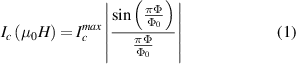
where  is the maximum critical current of the junction at zero field and
  is the magnetic flux quantum (fluxoid). To give some feeling for this behavior, we display simulated Fraunhofer patterns for lobe widths of 45 mT (J1) and 41 mT (J2) in figures 5(a) and (b) (blue curves).

Figure 5. I-V characteristics of the JJ devices (a) J1 at 2.5 K and (b) J2 1.2 K when applying out of plane magnetic field. The blue curve is the simulated Fraunhofer pattern (for lobe widths of 45 mT (J1) and 41 mT (J2)) for our devices dimensions, representing the relation between critical current Ic
and the applied magnetic flux. The outline (black) in (a) is at 1.6 µV while the outline (black and white) in (b) is at  V.
V.
Download figure:
Standard image High-resolution imageThe magnetic flux Φ is given by

Here, µ0
H is the external applied magnetic field in the interface plane of the junction, and  is the effective area of the junction. Using this description for our planar junctions, but with the applied field now perpendicular to the junction plane, we note that zero values for Ic
are reached when
is the effective area of the junction. Using this description for our planar junctions, but with the applied field now perpendicular to the junction plane, we note that zero values for Ic
are reached when  (with n an integer), so the width of the lobes
  is given by
  . Using the lobe width of 41 mT, this would lead to
  0.05 µm2. In overlap junctions, the area would be given by
  , with λL
the London penetration depth and w the width of the junction device. In lateral junctions one has to be careful with using that description. For the perpendicular fields of this geometry, λL
should be replaced by the Pearl length
, with λL
the London penetration depth and w the width of the junction device. In lateral junctions one has to be careful with using that description. For the perpendicular fields of this geometry, λL
should be replaced by the Pearl length  , but also the junction physics becomes different when the thickness d of the superconducting electrode isless than their London penetration depth, as is often the case for planar junctions. In particular, the description changes when the junction width w becomes smaller than the Josephson penetration length
  given by
  , with jc
being the (presumed homogeneous) critical current density of the junction. In this scenario, as has been discussed in numerous studies, the electrodynamics becomes non-local, and
, with jc
being the (presumed homogeneous) critical current density of the junction. In this scenario, as has been discussed in numerous studies, the electrodynamics becomes non-local, and  becomes independent of λL
and is solely determined by the geometry of the device [25, 31–34]. In our junctions, the thickness d of the MoGe layer (100 nm) is smaller than the bulk London penetration depth (580 nm). Consequently, the relevant penetration depth for the electrodes is given by the Pearl length Λ, calculated to be
becomes independent of λL
and is solely determined by the geometry of the device [25, 31–34]. In our junctions, the thickness d of the MoGe layer (100 nm) is smaller than the bulk London penetration depth (580 nm). Consequently, the relevant penetration depth for the electrodes is given by the Pearl length Λ, calculated to be  6.7 µm. This is significantly larger than the size of electrodes. Using the measured
  in J2 of about 0.1 mA through a cross-section of w = 250 nm and thickness t = 100 nm, we estimate
  to be
to be  97 nm. The junction width is actually somewhat larger than this, but it was discussed in [34] that non-local electrodynamics still apply. The simple answer for the lobe width in the interference pattern is that
  [25, 33, 35]. The lobe width
  mT then corresponds to a junction width of 265 nm, quite close to the actual number. We conclude that, under a perpendicular magnetic field, our junctions show the behavior expected for planar junctions.
5. Summary
In summary, we have grown high quality RuO2 nanostrips using the Selective Area (SA) growth on a TiO2 substrate and used these to fabricate planar Josephson junctions with the RuO2 strip as a weak link. We find these links not to behave as a normal metal; rather, the pair breaking effects are similar to what is found in weak ferromagnets such as CuNi and PdNi. The estimated coherence length of the weak link is about 12 nm. Moreover, the junctions behave as expected for planar junctions of such dimensions under the application of a magnetic field.
Acknowledgments
Technical support from M B S Hesselberth is gratefully acknowledged. This work is part of the research program of the Netherlands Organisation for Scientific Research (NWO). The work was supported by the Intel Corporation through Grant CG#38084911. The work was further supported by the EU COST action CA16218 'Nanocohybri' and by a grant from the Leiden-Delft Consortium 'NanoFront'.
Data availability statement
The data cannot be made publicly available upon publication because they are not available in a format that is sufficiently accessible or reusable by other researchers. The data that support the findings of this study are available upon reasonable request from the authors.
Appendix:
Appendix. A.1. A shorted junction
We also measured a device where voltage probes are shorted. Figure A1(a) shows that at the device becomes superconducting below the Tc of MoGe. The response of the device in magnetic field as expected shows the current hardly varies. This is in sharp contrast to the Fraunhofer-like pattern of junctions in figure 5.

Figure A1. (a) R(T) between 10 K to 2 K of a shorted -junction device. The device becomes superconducting below 6 K. (b) Color plot of I(µ0 H) of a shorted-junction device measured at 2 K. Field is applied out of plane to the device interface and varied from 0 to 150 mT. As expected current (I) stays almost constant under the whole range of field.
Download figure:
Standard image High-resolution imageAppendix. A.2 Closeup of a RuO2 nanostrip
Figure A2 shows a high resolution scanning eletron micrograph of two epitaxially grown RuO2 nanostrips of similar width of around 250 nm. In both cases, well defined crystal facets can be seen clearly. In (a) the width of the nanostrip is completely inside the trench. There are very small and thin crystals on SiOx but away from the trench. However, for (b) thin crystal shards are attached to the side along the length of the strip. A probable explanation is that RuO2 is known to grow on SiOx surface. The growth on SiOx is at a much slower rate. At the edge of the trench on both sides, these small crystals merged with the strip to give the above irregular growth.

Figure A2. High resolution close up SEM images of two RuO2 nanostrips.
Download figure:
Standard image High-resolution imageAppendix. A.3 Fitting IV characteristics
Figure A3 shows the I–V measurements at 2 K (in black) for both junctions J1 (a) and J2 (b). They were fitted by the following expression, derived from the work of Ambegaokar and Halperin (A-H)[26, 36]:

Figure A3. I − V Plots (in black) of J1 (a) and J2 (b) measured at 2 K along with their corresponding A-H fit (in red; see text). The inset shows the small interval of voltage where there is a deviation between the measurement and A-H fit.
Download figure:
Standard image High-resolution image
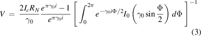
where  ,
,  , RN
is the normal resistance and I0 is a modified Bessel function. The A-H fits, given in figure A3 (in red) for both junctions at 2 K, look quite good. The insets show that there is a slight deviation in a small interval near 0 voltage, where the fit shows a sharper corner while the measurement is more rounded. We ascribe that to instrumental noise. The values for Ic
obtained in this way were plotted in figures 3(e) and (f).
, RN
is the normal resistance and I0 is a modified Bessel function. The A-H fits, given in figure A3 (in red) for both junctions at 2 K, look quite good. The insets show that there is a slight deviation in a small interval near 0 voltage, where the fit shows a sharper corner while the measurement is more rounded. We ascribe that to instrumental noise. The values for Ic
obtained in this way were plotted in figures 3(e) and (f).