
Abstract
We developed a low-temperature ohmic contact formation process for N-polar GaN surfaces. Specific-contact-resistances of 9.4 × 10⁻⁵ and 2.0 × 10⁻⁵ Ω cm2 were obtained using Ti/Al metal stacks on heavily-germanium-doped GaN films, which were deposited at 500 °C and 600 °C using a radical-assisted reactive sputtering method, respectively. The electrode sintering temperature was as low as 475 °C. Carrier concentrations for the 500 °C and 600 °C samples were 2.6 × 10²⁰ and 1.8 × 1020 cm−3, respectively. These results suggest that this method is highly effective in reducing the contact resistance of GaN devices with low thermal budgets.
Export citation and abstract BibTeX RIS

Content from this work may be used under the terms of the Creative Commons Attribution 4.0 license. Any further distribution of this work must maintain attribution to the author(s) and the title of the work, journal citation and DOI.
Gallium nitride (GaN) is more attractive as a power device than silicon (Si) owing to its great potential, such as a high critical electric field and electron mobility. 1,2) GaN power devices, such as MOSFETs, have been developed using high-quality GaN epitaxial wafers on freestanding GaN substrates. Devices with a high breakdown voltage and a low specific-on-resistance have been reported. 3–5) However, several issues still remain regarding the device fabrication processes for improving device characteristics and their practical application.
To further improve electrical characteristics, such as specific-on-resistance, it is necessary to reduce the ohmic contact resistance of the source and drain electrodes of the MOSFETs. Generally, to obtain low contact resistance, heavily-doped p- or n-type GaN epitaxial layers are prepared on the topmost GaN surface, and then metals are deposited on the surface, followed by high-temperature sinter annealing.
6–10) In the case of n-type GaN on the Ga-polar GaN surface (0001), it has been observed that the carrier concentration is over 1 × 1020 cm−3 using n-type dopants such as Si or germanium (Ge).
11) On the contrary, several GaN devices, such as vertical GaN power devices,
5,12,13) and N-polar high-electron-mobility transistors,
14,15) require an ohmic contact on the N-polar surface  For vertical power devices, it is typically necessary to make contact on the N-polar GaN surface, i.e., the backside of the GaN
  substrate with a carrier concentration of around 1 × 1018 cm−3 directly.
16) In addition, a critical issue is that the GaN substrate should be thinned from the backside surface by grinding and polishing
17,18) to reduce series resistance as well as thermal resistance of the substrate. We have experimentally confirmed that it becomes difficult to obtain low contact resistance on the polished N-polar GaN surface without higher-temperature sintering than 600 °C. However, for the backside (N-polar surface) fabrication processes, lower-temperature processing, typically less than 600 °C is required to avoid degradation of device performances, since the main device structure has already been fabricated on the upside Ga-polar surface before the backside contact formation. Therefore, it is necessary to establish low-temperature backside ohmic contact formation processes to obtain low contact resistance.
substrate with a carrier concentration of around 1 × 1018 cm−3 directly.
16) In addition, a critical issue is that the GaN substrate should be thinned from the backside surface by grinding and polishing
17,18) to reduce series resistance as well as thermal resistance of the substrate. We have experimentally confirmed that it becomes difficult to obtain low contact resistance on the polished N-polar GaN surface without higher-temperature sintering than 600 °C. However, for the backside (N-polar surface) fabrication processes, lower-temperature processing, typically less than 600 °C is required to avoid degradation of device performances, since the main device structure has already been fabricated on the upside Ga-polar surface before the backside contact formation. Therefore, it is necessary to establish low-temperature backside ohmic contact formation processes to obtain low contact resistance.
To obtain a good ohmic contact, forming additional heavily-doped n-type GaN films on the surface is effective. However, epitaxial growth of n-type GaN on N-polar surfaces using metal-organic vapor phase epitaxy is very difficult because it requires a high growth temperature (>1000 °C). 19,20) Ion implantation technique is another method to form heavily-doped n-type, but it also requires higher-temperature activation annealing (>1000 °C). 21) Then, we focused on a sputtering method as a growth technology. Recently, a sputtering method for the III–V compound semiconductor growth has been remarkably developed. 22–24) And it is expected that this technique will be applied to various GaN devices, not only for power devices but also for HF devices. There are several advantages of using this sputtering technique. One of the key advantages is the availability of low-temperature deposition, such as around 700 °C of the substrate-temperature. This temperature is particularly attractive for vertical-type MOSFETs, as mentioned above. The second advantage is that it is hydrogen-free in the sputtering sources and ambient gases, which makes it possible to grow n-type GaN films without inducing magnesium (Mg) deactivation by hydrogen (formation of the MgGa-H complex). 25,26) The third advantage is the heavy doping ability. Since this method is performed in a nonequilibrium state, it is suitable for the realization of heavily-doped GaN films with a higher carrier concentration as an ohmic contact layer. However, there have been few studies on the application of sputtering deposition for contact layers, particularly for N-polar surfaces. 24)
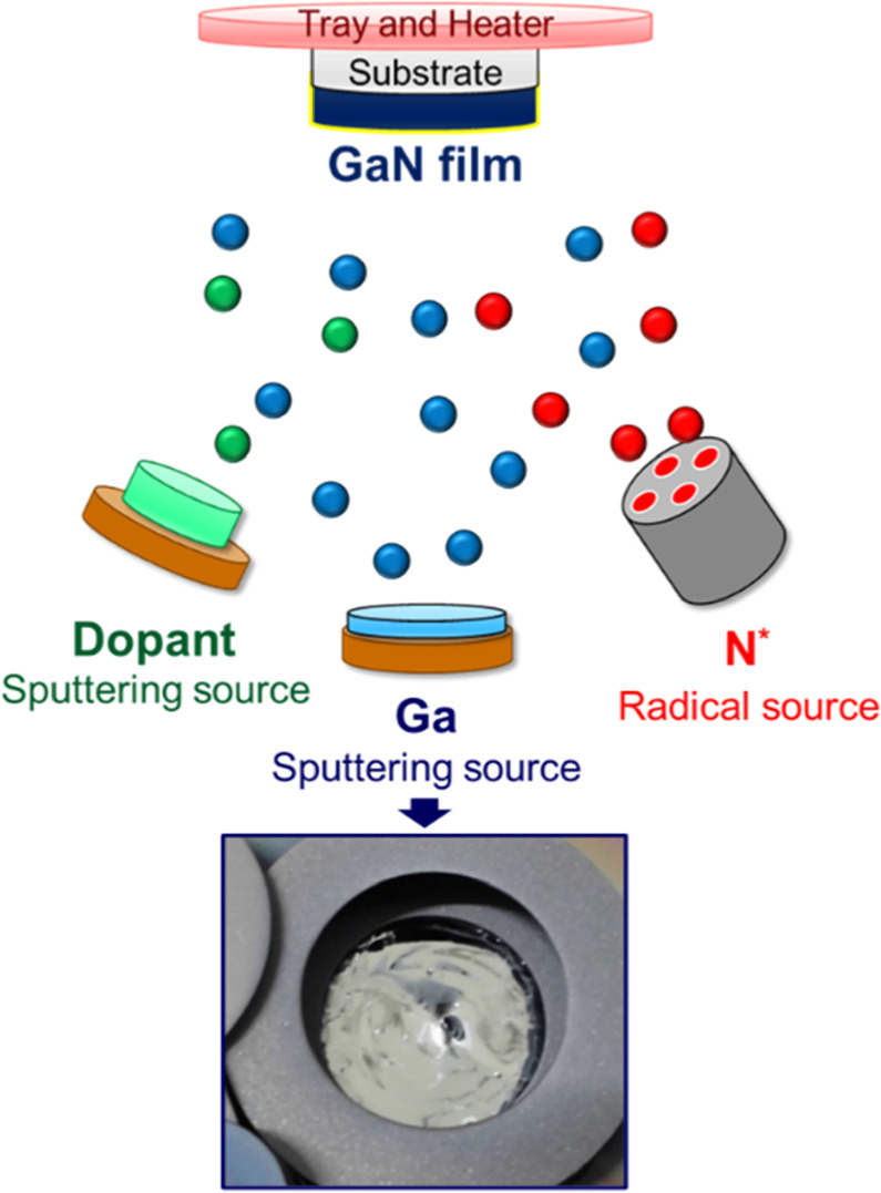
In this study, we investigated the low-temperature growth and heavily-Ge-doped n-type GaN films on an N-polar GaN surface using radical-assisted reactive GaN sputtering and evaluated their electrical properties. The temperatures were equal to or less than 600 °C which is sufficiently low for the thermal budgets of MOSFETs. In this method, liquid-phase Ga and a nitrogen radical (N*) gun were utilized as the sputtering sources, and the Ge target was employed as an n-type dopant. A schematic view of the equipment and a photograph of the Ga source are shown in Fig. 1. Each source was sputtered with an Ar or N2 gas plasma generated by a DC or RF generator. The sputtered Ga and Ge particles, along with N*, reached the substrate surface and underwent chemical reactions. Subsequently, a GaN film formed on the substrate surface. The equipment configuration is conventional, making it easy to use and suitable for manufacturing.

Fig. 1. Schematic view of the GaN sputtering equipment and a picture of the liquid-phase gallium (Ga) target as the sputtering source. The sample tray and heater unit were located on the upper side, while the sputtering sources, such as Ga and germanium (Ge), and the radical source (nitrogen radical) were at the bottom in the vacuum chamber.
Download figure:
Standard image High-resolution imageThe substrates used in this study were N-polar semi-insulating GaN (SI-GaN) grown by hydride vapor phase epitaxy with a thickness of 420 μm in order to prevent the current spreading to the substrates and evaluate the electrical properties of only GaN films precisely. First, to simulate the actual fabrication processes of MOSFETs, the N-polar surfaces were thinned to a depth of approximately 50 μm from the surface by grinding and were mirror-polished by chemical mechanical polishing. The samples were then cleaned with several organic solvents and acid solutions, rinsed and dried. Subsequently, GaN sputtering was performed on the N-polar SI-GaN substrates. The typical deposition conditions are as follows: the Ge sputtering power was varied as sputtering parameters using a pulsed DC generator. The Ge/Ga sputtering power ratio was varied from 0 to 0.15 under constant Ga sputtering power. The SI-GaN substrate temperatures were 500 °C and 600 °C. The target deposition thickness was 100 nm, and the deposition time was approximately 16 min. To investigate the crystalline quality and Ge doping concentration [Ge] of the GaN films, cross-sectional transmission electron microscopy (TEM) and secondary ion mass spectrometry (SIMS) were performed. For electrical characterization, Hall-effect 27) and circular transmission line method (c-TLM) 28–30) devices were fabricated on the GaN films. Figure 2 shows a schematic of the fabricated device structure. The process flow for device fabrication is as follows: after GaN sputtering deposition, 500 nm-thickness-SiO2 films were deposited by plasma-enhanced chemical vapor deposition onto the GaN film surfaces. Next, photoresist patterns were formed using photolithography on the SiO2 films. Subsequently, wet-etching using an HF solution was performed to remove the exposed SiO2 films, and the surfaces of the GaN films were partially exposed. Next, after removing the photoresist mask, dry-etching of the GaN films was performed to form device patterns using inductively coupled plasma reactive ion etching. After dry-etching, the exposed GaN films were removed, and the SI-GaN substrates were partially exposed. Next, the second photoresist patterns were formed, and wet-etching was performed to remove the exposed SiO2 films to create an ohmic contact area. Subsequently, a Ti/Al metal stack was deposited using an electron beam evaporator, and a lift-off process was performed to remove the metal stack on the photoresist using an organic solution. Finally, 475 °C sintering was performed in N2 ambient for 5 min to obtain the ohmic contact by rapid thermal annealing. Such a low sintering temperature was chosen to suppress the influence of the Ga-polar front-end device structure on future GaN-MOSFET device fabrication processes. The Hall-effect devices had cloverleaf shapes in which the current spreading region was 1 mm × 1 mm. The c-TLM devices also contained 6 rings in which the outer diameter was constant at 600 μm, and gap lengths (d) among metals were changed from 20 to 150 μm. After the device fabrication, Hall-effect measurements were performed using the Van der Pauw method under an AC magnetic field of 0.512 T and a current of 0.1 mA at RT. The c-TLM measurements were also performed at RT.
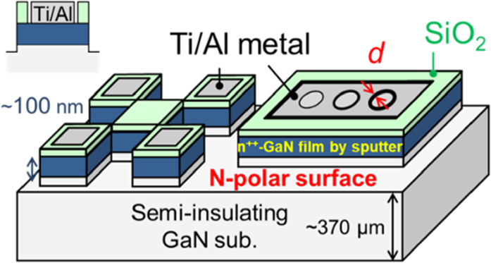
Fig. 2. Schematic of the device structures for the Hall-effect and circular-TLM measurements using the GaN films deposited by sputtering on a semi-insulating GaN substrate.
Download figure:
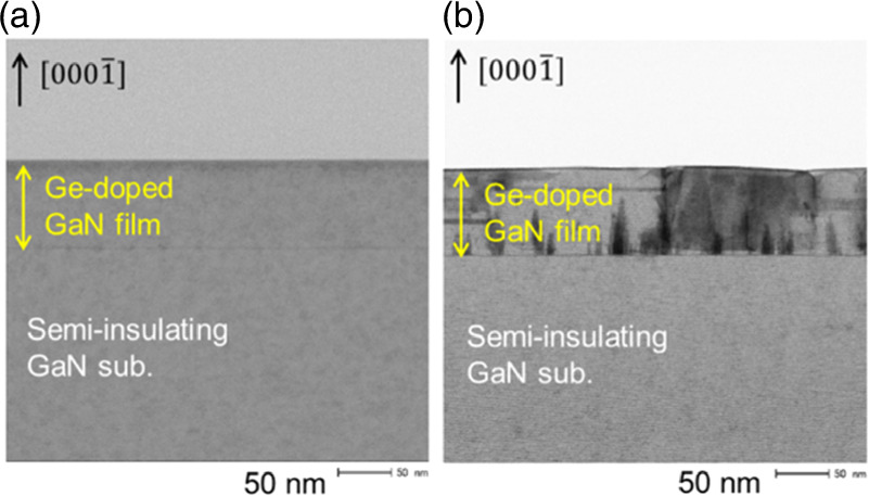
Standard image High-resolution imageFigure 3 shows the cross-sectional TEM images of the Ge-doped GaN films deposited at 600 °C and 500 °C with a Ge/Ga sputtering ratio of 0.11. The measured thickness of the GaN film in each sample was approximately 90 nm. As shown in Fig. 2(a), the contrast of the film deposited at 600 °C was almost similar to the SI-GaN substrate, confirming that the film was grown totally epitaxially on the SI-GaN substrate. On the other hand, that of the film deposited at 500 °C shown in Fig. 2(b) was different from the SI-GaN substrate. It was found that the film was epitaxial in most parts. However, it was considered that it included many defects such as stacking faults and inversion domains, because the migration of sputtered Ga was not enough on the plane surface of the substrate due to such a low-temperature condition. A detailed study on these crystalline defects will be conducted in the future.

Fig. 3. Cross-sectional TEM images of the GaN films at (a) 600 °C and (b) 500 °C deposited at a Ge/Ga sputtering power ratio of 0.11 on a semi-insulating GaN substrate.
Download figure:
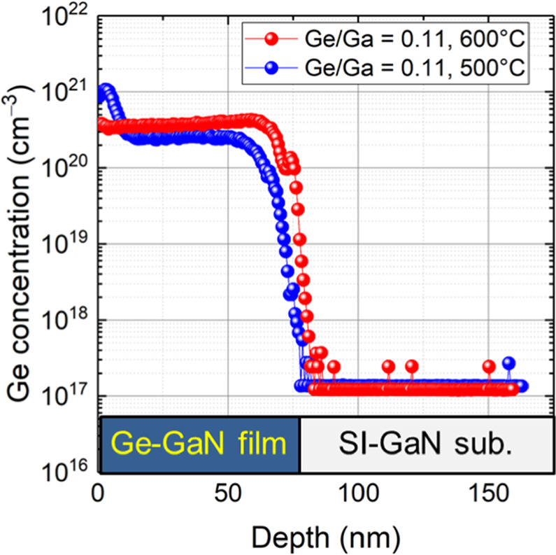
Standard image High-resolution imageFigure 4 shows the [Ge] in the GaN films deposited at 600 °C and 500 °C analyzed by SIMS. From the result, Ge was surely doped in the GaN films, and [Ge] at 600 °C and 500 °C were 3.9 × 10²⁰ and 2.5 × 1020 cm−3, respectively. On the other hand, the carbon concentration [C], which compensates donors was typically below 1 × 1019 cm−3. Therefore, the Ge-doped GaN films must be heavily-doped n-type layers.

Fig. 4. Ge concentrations of the GaN films at 600 °C (red dots) and 500 °C (blue dots) deposited at a Ge/Ga sputtering power ratio of 0.11, analyzed by SIMS.
Download figure:
Standard image High-resolution imageNext, the Hall-effect measurements provided the sheet resistance (Rsh_Hall), Hall mobility (μ), and carrier concentration (n), as summarized in Table I. In the case of 500 °C deposition, an increase in the Ge/Ga sputtering power ratio, resulted in a monotonically increasing n, indicating heavier Ge doping with an increasing Ge/Ga power ratio. For Ge/Ga = 0.11, n of the sample deposited at 500 °C was 1.7 × 1020 cm−3, similar to that at 600 °C (1.8 × 1020 cm−3). It was considered that the carrier concentration might be limited to around 1.8 × 1020 cm−3 for N-polar GaN surface, because the excess of Ge was not located at the Ga-site as an n-type dopant, but at the N-site or interstitial. Furthermore, Rsh_Hall decreased monotonically, and μ exhibited a slight decrease with an increasing Ge/Ga ratio. This result indicates that Ge-doped GaN films deposited at lower temperatures, such as 500 °C effectively function as heavily-doped n-type GaN. As the [C] in the GaN films were less than 1 × 1019 cm−3, the compensation ratio was less than 10%. Therefore, the carrier concentration of the GaN film at 500 °C was roughly 70% active against [Ge], as indicated by the SIMS results.
Table I. Parameters for heavily-Ge-doped n-type GaN films under various sputtering conditions evaluated from the Hall-effect and the circular-TLM measurements.
| Sputtering conditions | Hall-effect devices | Circular-TLM devices | |||||
|---|---|---|---|---|---|---|---|
| Temperature (°C) | Ge/Ga ratio | Rsh_Hall(Ω/sq) | μ (cm2/V·s) | n (cm−3) | Lt(μm) | Rsh_TLM(Ω/sq) | ρc(Ω·cm2) |
| 600 | 0.11 | 48 | 79 | 1.8 × 10²⁰ | 6.2 | 53 | 2.0 × 10⁻⁵ |
| 500 | 0 | 6200 | 46 | 8.5 × 10¹⁸ | 1.3 | 7200 | 1.3 × 10⁻⁴ |
| 500 | 0.07 | 240 | 64 | 4.5 × 10¹⁹ | 21 | 150 | 6.9 × 10⁻⁴ |
| 500 | 0.11 | 90 | 45 | 1.7 × 10²⁰ | 15 | 78 | 1.7 × 10⁻⁴ |
| 500 | 0.15 | 60 | 44 | 2.6 × 10²⁰ | 14 | 51 | 9.4 × 10⁻⁵ |
Subsequently, current−voltage (I−V) characteristics were measured using c-TLM devices. Figure 5(a) illustrates the I−V curves of the GaN films at d = 80 μm deposited at different Ge/Ga ratios from 0 to 0.15 at 500 °C. For Ge/Ga ratio = 0, the GaN film exhibited high resistivity, with almost no current in the voltage range from −50 to 50 mV. Conversely, for Ge/Ga ratios from 0.07 to 0.15, the I−V curves exhibited ohmic characteristics, and the current clearly increased with an increasing Ge/Ga ratio. The relationship between the gap length (d) and the total resistance (RT) is plotted in Fig. 5(b). Several parameters, such as the transfer length (Lt), sheet resistance (Rsh_TLM), and specific contact resistance (ρc) were calculated using the c-TLM formulas:


and

where C is the correlation factor used to correct the plots to a linear form, and r is the radius of the outer ring, with r = 600 μm in this experiment. Then, RT and d are expressed as linear functions, as shown in Equation (3). RT was calculated from the I−V characteristics at V = 20 mV. RT increased monotonically with an increase in d, as shown in Fig. 5(b). RT decreased at the same gap lengths with an increase in the Ge/Ga ratio. From these plots, the parameters were calculated as Lt = −(the x-axis intercept)/2, Rsh_TLM = (the slope) × 2πr, and ρc = Rsh_TLM × Lt 2 and the summary is also shown in Table I. Firstly, the properties of the GaN film at 600 °C with a Ge/Ga ratio = 0.11 were excellent, and the ρc was 2.0 × 10⁻⁵ Ω cm2, which was the lowest resistance among all samples. On the other hand, in the case of 500 °C deposition, the ρc also decreased with an increase in the Ge/Ga ratio. The ρc at Ge/Ga ratio = 0.15, which was the most heavily-doped sample, was 9.4 × 10⁻⁵ Ω cm2. Comparing 600 °C and 500 °C with a Ge/Ga ratio = 0.11, the ρc degraded for the lower deposition temperature, thought to be due to lower crystallinity. However, a ρc of the order of 10−5 Ω·cm2 was surely obtained by heavily-Ge-doping even at 500 °C. Furthermore, the Rsh_TLM decreased with an increasing Ge/Ga ratio, and this trend was similar to that of Rsh_Hall. The Rsh_TLM at Ge/Ga ratio = 0.15 was 51 Ω/sq. It should be noted that high sintering temperatures were not used. In this study, we fixed sintering conditions at 475 °C for 5 min. Further optimization of sintering conditions will lead to lower ρc in the future.

Fig. 5. (a) I−V characteristics for the GaN films at the gap length (d) of 80 μm of circular-TLM devices under various Ge/Ga sputtering power ratio conditions. (b) Total resistances of the GaN films as a function of the gap lengths at 20 mV under various Ge/Ga sputtering power ratio conditions.
Download figure:
Standard image High-resolution image
In conclusion, the electrical properties of heavily-Ge-doped n-type GaN films were investigated on N-polar GaN surfaces deposited using low-temperature GaN reactive sputtering. We employed a low temperature 475 °C for sintering to achieve low thermal budgets. The carrier concentrations (n) increased, and the specific-contact-resistances (ρc) decreased with increasing Ge/Ga sputtering ratios. Under the Ge/Ga ratio = 0.15 and 500 °C, the n and the ρc were 2.6 × 1020 cm−3 and 9.4 × 10⁻⁵ Ω cm2, respectively. In the case of higher temperature (600 °C) deposition, the lowest ρc obtained was 2.0 × 10⁻⁵ cm2. Thus, it was concluded that the heavily-Ge-doped n-type GaN films fabricated using the sputtering technique contributed to the realization of a low specific-contact-resistance on the N-polar GaN surface.
Acknowledgments
This work was supported by MEXT-Program for Creation of Innovative Core Technology for Power Electronics Grant No. JPJ009777. The authors thank Dr Masahiro Horita from Nagoya University and Mr Taehui Lee who was a graduate student at Nagoya University for their valuable discussions and analyses.