

Abstract
Quantum wells in InGaAs/AlGaAs with (110) orientation are attractive as active layers in spin-controlled lasers with circularly polarized emission, while the spin relaxation time is expected to be larger than for (100)-oriented layers. However, the hitherto reported recombination lifetimes (40 ps) and spin relaxation times (440 ps) of (110) InGaAs/AlGaAs structures are insufficient. Here it is shown that higher growth temperatures and higher V/III beam equivalent pressure ratios than previously used in crystal growth by molecular beam epitaxy lead to recombination and spin relaxation times in the nanosecond range at RT, meeting the requirements for application in spin lasers.
Export citation and abstract BibTeX RIS

Content from this work may be used under the terms of the Creative Commons Attribution 4.0 license. Any further distribution of this work must maintain attribution to the author(s) and the title of the work, journal citation and DOI.
Semiconductor lasers that emit circularly polarized light, based on meta surfaces, 1,2) photonic crystals 3) or electron spins, 4,5) have gained attention for their potential use in data communication and sensing applications. In a spin-controlled semiconductor laser (spin laser), a circularly polarized output is generated due to the spin-dependent optical selection rules. This enables reduction in the threshold current 6) as well as switching of the output polarization by controlling the spin orientation. 7–9) To achieve laser emission with high circular polarization, it is necessary to maintain electron spin polarization during carrier recombination in the active layer. This requires the spin relaxation time (τs) to be at least as long as the recombination lifetime (τr) of the active layer, which is typically a few nanoseconds. Spin lasers have used GaAs bulk, 10) InGaAs quantum wells (QWs) 11) and InAs quantum dots 12) on (100) GaAs substrates as active layers. Among these, the longest τs is several hundred picoseconds for InAs quantum dots at 200 K. 13) On the other hand, (110)-oriented QWs are promising for the active layers as they exhibit long τs at RT due to the suppression of D'yakonov–Perel' (DP) spin relaxation. 14) The τs and τr of (110) QWs reported in the literature so far are summarized in Table I. Long τs of a few nanoseconds were first demonstrated for the most fundamental material system, (110)-oriented GaAs/AlGaAs. 15,16) Subsequently, circularly polarized lasing with high circular polarization was demonstrated in a vertical cavity surface emitting laser with (110) GaAs/AlGaAs active layers at RT, taking advantage of the long τs. 17) In terms of τr, an indicator of crystal quality, high-quality (110) GaAs/AlGaAs QWs with τr in the nanosecond range have been demonstrated using optimized growth conditions for homoepitaxial growth on (110) GaAs substrates. 18–22) InGaAs, a ternary semiconductor, is more attractive than GaAs for the active well layer due to its tunable wavelength in the desired range, improved differential gain and reduced threshold current resulting from the reduced density of states. 23) However, there are few reports on τr and τs for (110) InGaAs QWs. 24–26) In a study of InGaAs/InAlAs QWs on (110) InP substrates with rough surfaces having faceted hillocks, τs was found to be 0.7–1.0 ns, 26) which is only about one-third of the value for (110) GaAs/AlGaAs QWs. This is due to the narrow bandgap of the system (0.8 eV) inducing Elliott–Yafet (EY) spin relaxation at RT. 27) On the other hand, InGaAs/(Al)GaAs QWs on a (110) GaAs substrate, utilized as active layers in lasers for short-range optical communication and sensing applications, are expected to have a longer τs due to the suppression of EY spin relaxation. This is because the bandgap (1.2–1.4 eV) of the system is larger than that of (110) InGaAs QWs grown on (110) InP substrates. Therefore, InGaAs QWs on (110) GaAs substrates are attractive as active layers for spin lasers. However, the τr demonstrated so far for (110) InGaAs/(Al)GaAs QWs has been as short as 40 ps at RT, indicating that the crystal quality is not optimal. 24,25) Additionally, the obtained τs was approximately 440 ps, significantly shorter than expected due to low crystal quality. Therefore, improving the crystal growth of (110) InGaAs/AlGaAs is crucial for achieving τr and τs in the nanosecond range, as required for the active layer of a spin laser.
Table I. Summary of the wavelength, recombination lifetime (τr) and spin relaxation time (τs) at RT reported in quantum wells grown on (110) III–V substrates.
| References | Well/barrier materials | Features of material systems | τr (ns) | τs (ns) |
|---|---|---|---|---|
| 15–17, 21, 22 | (110) GaAs/AlGaAs on GaAs substrates | Narrow wavelength band (800–850 nm); lattice-matched system | > 1 | > 1 |
| 26 | (110) InGaAs/InAlAs on InP substrates | Telecom wavelength (1.55 μm); lattice-matched system | > 1 | 0.7–1.0 |
| 24, 25 | (110) InGaAs/GaAs on GaAs substrates | Wide wavelength band (900–1100 nm); strained system | 0.04 | 0.4 |
| This work | (110) InGaAs/AlGaAs on GaAs substrates | Wide wavelength band (810–1100 nm); strained system | > 1 | 1.0–1.2 |
Here we show that recombination lifetimes and spin relaxation times in the nanosecond range can be obtained in (110) InGaAs/AlGaAs QWs on (110) GaAs at RT by using higher growth temperatures and higher V/III beam equivalent pressure (BEP) ratios than previously used in crystal growth by MBE. Since these results meet the required values for the active layers, it is expected that spin lasers using (110) InGaAs/AlGaAs QWs could achieve circularly polarized lasing at RT.
Five-period In0.08Ga0.92As/Al0.1Ga0.9As QWs with an InGaAs well thickness of 9 nm were grown on semi-insulating (110) GaAs substrates by MBE. In order to optimize the crystal quality, the growth temperature (Tg) was varied from 440 °C to 500 °C and the BEP ratio (Rf) of the group V and III elements was varied from 80 to 240. A total of eight samples were fabricated without intentional doping. In previous studies, a short τr of 40 ps was reported in InGaAs/(Al)GaAs on (110) GaAs with a Tg of 440–455 °C and As4/III BEP ratios of 25–80. 24,25) Such an extremely short τr means that the sample has many defects, such as vacancies in group III and V atoms that act as non-radiative recombination centers, so it is necessary to find growth conditions that suppress the formation of defects. Since both Ga and As atoms coexist on non-polar (110) GaAs surfaces, the incorporation coefficient of the As atoms during growth of GaAs decreases to about one-half of that on a (100) surface, 19) which results in As vacancies due to lack of As atoms on the growth surface. To improve this low As incorporation, in previous studies crystal growth of (110) InGaAs/AlGaAs QWs was conducted at low temperatures, which can lead to the generation of vacancies of the group III atoms due to their reduced surface migration. Therefore, we investigated a higher BEP ratio range and a higher growth temperature than in previous studies to control the As deficiency and surface migration of group III atoms on the growth surface. Moreover, instead of As4 we used As2 as the As species because As2 is expected to have twice the As incorporation efficiency of As4, 19) which helps to suppress As deficiency. We note here that since the detection sensitivity of As2 by an ion gauge is about one-fifth of that for As4, an As2/III BEP ratio of 80 means that As atoms are irradiated five times more than for the As4/III BEP ratios used in previous work. 24,25)
The surfaces of the samples are all mirror-like, and the surface average roughness evaluated by atomic force microscopy (AFM) is less than 0.4 nm for all samples, implying sufficient quality for optical measurement of the samples. A typical AFM image of the surface morphology with an average surface roughness of 0.14 nm is shown in Fig. 1(a), where a one to two monolayer step-terrace structure is observed. The X-ray diffraction measurements (333) reciprocal space mapping) show that the in-plane lattice constant of the InGaAs matches that of the AlGaAs barrier layer. Since the unit cell of bulk InGaAs is about 0.6% larger than that of AlGaAs, this indicates that the InGaAs well layers are strained without lattice relaxation. Typical reciprocal lattice mapping data for a sample grown with a Tg of 480 °C and an Rf of 200 are shown in Fig. 1(b). The satellite peaks derived from the five-period QWs are aligned along the Q[110] axis, indicating that InGaAs layers are not lattice-relaxed.
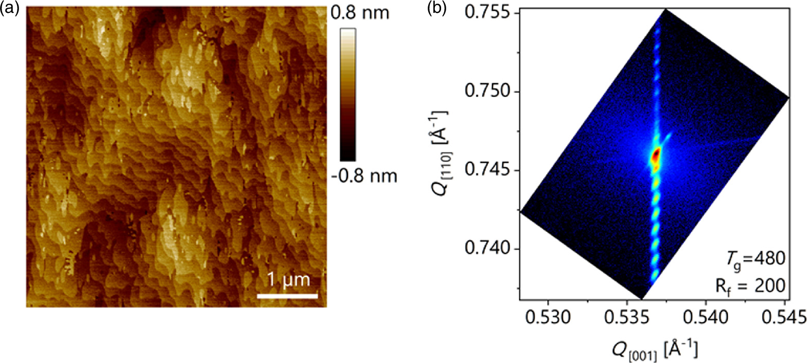
Fig. 1. (a) Atomic force microscope images with a scan size of 5 μm × 5 μm for the sample grown at a temperature (Tg) of 480 °C and a V/III BEP ratio (Rf) of 200, having an average surface roughness of 0.14 nm. (b) The X-ray diffraction pattern [(333) reciprocal space map] for the same sample as in (a).
Download figure:
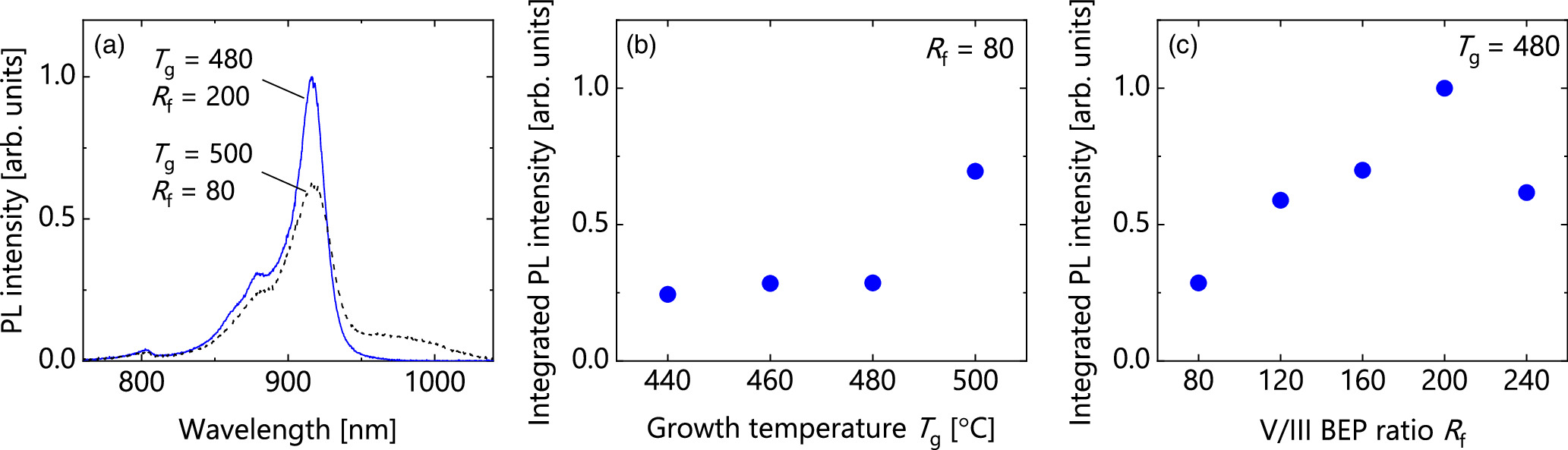
Standard image High-resolution imageNext, we describe the continuous-wave photoluminescence (PL) characteristics of the samples measured at RT. A diode-pumped solid-state laser with an optical power of 1 mW at 532 nm was used as the excitation source, and a fiber spectrometer was used for spectral measurements. Figure 2(a) displays the PL spectra of two samples [(Tg, Rf) = (480, 200) and (500, 80)]. In both PL spectra, three peaks are observed at wavelengths of 803 nm, 879 nm and 916 nm. These correspond to the bulk conduction band to VB transition in the AlGaAs barrier layers, the electron–light-hole transition and the electron–heavy-hole transition for the quantized ground state of the quantum well layers, respectively. The wavelengths are in approximate agreement with the calculated values.

Fig. 2. (a) PL spectra obtained at RT for the two samples [(Tg, Rf) = (480, 200) and (500, 80)]. The PL intensity integrated between 910 nm and 930 nm is plotted as a function of (b) growth temperature Tg and (c) BEP ratio Rf.
Download figure:
Standard image High-resolution imageThe growth temperature dependence of the PL intensity integrated at 910–930 nm in each PL spectrum is shown in Fig. 2(b). The data are normalized to the PL intensity at a Tg of 480 °C and an Rf of 200, which exhibited the largest PL intensity among all samples. The PL intensity increases with increasing Tg. However, although the PL intensity increases by a factor of two between Tg = 480 °C and 500 °C, a broad weak PL in the 500 °C sample was also observed at the long-wavelength side of the electron–heavy-hole transition with a wavelength range of 950–1000 nm [see Fig. 2(a)]. Such additional PL is attributed to the inhomogeneous In composition caused by the aggregation of In atoms due to high-temperature growth. Next, we discuss the Rf dependence of PL characteristics at a Tg of 480 °C, shown in Fig. 2(c). The PL intensity increases with increasing Rf, with the maximum PL intensity at Rf = 200. Since the same number of photoexcited carriers were generated in all PL measurements, the measured PL intensities qualitatively reflect the carrier-to-photon conversion efficiency, namely quantum efficiency. Thus, we conclude that Figs. 2(b) and 2(c) show that high growth temperatures and high BEP ratios are important for increasing the quantum efficiency.
To investigate the recombination lifetimes, which indicate quantum efficiency at RT, and determine the spin relaxation times of the samples, circularly polarized time-resolved PL (TRPL) measurements with integration at a wavelength of 910–930 nm were performed at RT. Since the defect-derived non-radiative recombination rate of carriers is usually several orders of magnitude faster than the radiative recombination rate at RT, the RT recombination lifetime is approximately equal to the non-radiative recombination lifetime, which means that the longer the RT recombination lifetime, the fewer defect-derived non-radiative recombination centers and the higher the quantum efficiency. Owing to the spin-dependent optical selection rules, electrons with spin perpendicular to the plane of the QWs are excited into the conduction band by right circularly polarized (σ+) excitation pulses. These electrons subsequently decay radiatively into the VB. The resulting PL is partially circularly polarized, reflecting the degree of perpendicular spin polarization of the recombination electrons. Right  and left
  circularly polarized components of the PL, which reflect down and up spin electron densities in the conduction band, respectively, were converted separately to orthogonal linearly polarized light using a quarter-wave plate and a linear polarizer. The PLs were measured with a 25 cm monochromator and a streak camera. Typical TRPL data for the sample with Tg of 480 °C and Rf of 200 are shown in Fig. 3. The spin polarized electrons in the conduction band are generated by the circularly polarized excitation pulse at time t = 0. The intensities of both polarized PLs are maintained over nanoseconds, indicating that this sample has a long recombination lifetime. In addition, the difference in PL intensity between both polarizations is maintained for about 1 ns, indicating that the spin relaxation time is also large. τr is extracted by fitting
  with a single exponential decay function ∼
 From the calculated temporal circular polarization
  of the PL, we obtain τs by using a fitting function defined as
  28) Here, we should note that the hole spins are practically unpolarized due to their short spin relaxation times.
29) The circular polarization observed for the PL therefore comes from the spin polarization of electrons in the conduction band.
28) Here, we should note that the hole spins are practically unpolarized due to their short spin relaxation times.
29) The circular polarization observed for the PL therefore comes from the spin polarization of electrons in the conduction band.

Fig. 3. Typical results of polarization- and time-resolved PL decay measured at RT for the sample grown at a Tg of 480 °C and Rf of 200. The circular polarization (Pc, green line) is given by  where
where  (black line) and
  (red line) represent the right and left circularly polarized PL components under σ+ excitation, respectively. The periodic fine oscillations of
 and
and  (blue line) are due to the etalon effect in the measurement system.
Download figure:
Standard image High-resolution imageFigures 4(a) and 4(b) show the Tg and Rf dependence of τr, respectively. The τr obtained for a Tg of 440 °C and an As2 Rf of 80 is 0.4 ns, which is about one order of magnitude longer than that for same Tg and Rf but using As4 as the As species. 24,25) Note that the detection sensitivity of As2 by the ion gauge is about one-fifth of that for As4. This indicates that irradiating a large number of As2 atoms is very effective in increasing the recombination lifetime – in other words, in suppressing the formation of non-radiative recombination centers. As4 with a BEP ratio of 80 does not have enough As atoms incorporated at the growth surface, resulting in As vacancy-derived defects that can act as non-radiative recombination centers [see Fig. 5(a)]. The monotonically increasing τr up to a BEP ratio of 200 in Fig. 4(b) also indicates that the As vacancy-derived defects are the origin of the non-radiative recombination centers. The likely reason for the shorter τr at a BEP ratio of 240 is that excess As atoms are incorporated into the interstitial lattice and act as non-radiative recombination centers, as shown in Fig. 5(b). Raising Tg also increases τr. Increasing the growth temperature lowers the incorporation efficiency of As atoms during growth, resulting in non-radiative recombination centers derived from As vacancies, while promoting the migration of group III atoms at the growth surface and suppressing the generation of group III vacancies that also act as non-radiative recombination center [see Fig. 5(c)]. The fact that the recombination lifetime increases with increasing growth temperature suggests that it is also important to reduce the group III atom vacancies to obtain a long recombination lifetime, which suggests that higher growth temperatures are effective for this purpose. However, surface morphology based on AFM measurements shows that small facets are formed on the surface at a Tg of 500 °C, which results in a reduction in the mirror reflectivity of the laser. Therefore, to obtain a flat surface and recombination lifetime in the nanosecond range, which is required for the laser active layer, we conclude that the growth conditions should be Tg ≥ 480 °C and As2 Rf ≥ 120, with the best result obtained at an Rf of 200. We also point out that high-quality crystals with recombination lifetimes in the nanosecond range (i.e. the PL signals are maintained over a long time) enable accurate evaluation of the long electron spin relaxation time of the (110)-oriented InGaAs/AlGaAs QWs.
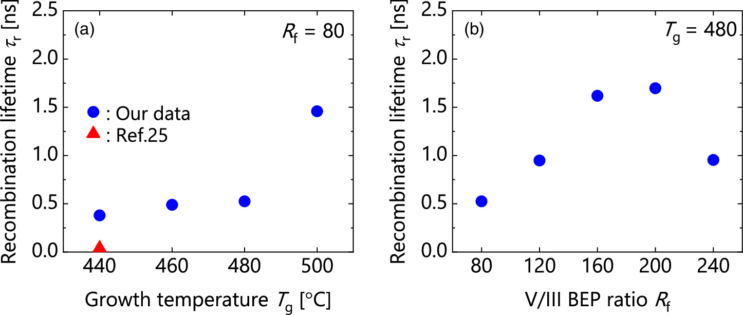
Fig. 4. Dependence of the recombination time at RT on the growth temperature Tg (a) and the BEP ratio Rf (b).
Download figure:
Standard image High-resolution image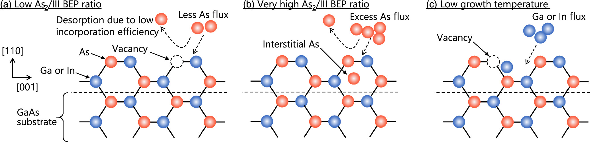
Fig. 5. Schematic drawings illustrating the formation of crystal defects during crystal growth on the GaAs (110) surface (side view). (a) Under a low BEP ratio, where only a small fraction of the irradiated As flux is incorporated into the crystal due to the low incorporation efficiency of As atoms, vacancies can be formed in the As sites. (b) In the situation of very high BEP ratio, excess As atoms can be incorporated into the interstitial lattice due to the irradiation of excess As flux. (c) At low growth temperature, vacancies can be formed in group III sites due to insufficient surface migration of group III atoms (Ga or In atoms).
Download figure:
Standard image High-resolution imageFigures 6(a) and 6(b) show the dependence of τs on the growth temperature and BEP ratio. The exposure time of the streak camera was adjusted to improve the signal-to-noise ratio of the decay curve for circular polarization in samples with τs longer than τr. This resulted in accurate values of τs within an error of 10% for all samples. The measured τs is independent of growth conditions and approximately 1 ns for all samples. This value is several tens of times longer than that of the (100)-oriented InGaAs/AlGaAs on GaAs substrates. 30) These results meet the criteria for application to the active layer in spin lasers. The reason for such a long spin relaxation time is that DP spin relaxation is suppressed, similar to (110) GaAs/AlGaAs QWs. 14) However, the τs obtained for (110) InGaAs/AlGaAs QWs is approximately half of that for (110) GaAs/AlGaAs QWs, 15) suggesting that a different spin relaxation mechanism is more enhanced in InGaAs/AlGaAs QWs than in GaAs/AlGaAs QWs. The EY mechanism 27) is a potential candidate for enhancing the spin relaxation due to the smaller bandgap, larger spin split-off energy and lighter effective mass of electrons in InGaAs compared with GaAs. In the EY mechanism, τs is proportional to the scattering time, which depends on electron scattering originating from polar optical phonons as well as crystal imperfections such as defects (non-radiative recombination centers) in InGaAs. This indicates that the scattering times for all samples remain almost constant regardless of the growth conditions. Therefore, electron scattering from non-radiative recombination centers makes a much smaller contribution to scattering time in our high-quality samples than polar optical phonon scattering at RT. On the other hand, the short τr of 40 ps reported in Ref. 25 suggests the existence of numerous non-radiative recombination centers, which can affect the scattering time. As a result, reducing the scattering time leads to a short τs of 440 ps in Ref., 25 which is less than half the value obtained from our samples. Even the sample with the shortest τr of 0.4 ns (Tg = 480 °C and As2 Rf = 80) achieved a long τs of 1 ns. This indicates that a crystal with a τr of several hundred picoseconds is necessary to achieve a τs in the nanosecond range.

Fig. 6. Dependence of the spin relaxation time at RT on the growth temperature Tg (a) and the BEP ratio Rf (b).
Download figure:
Standard image High-resolution image
In summary, we have systematically investigated the dependence of the recombination lifetime and spin relaxation time on crystal growth conditions in (110)-oriented InGaAs/AlGaAs QWs. It is found that recombination lifetimes can be improved drastically and reach the nanosecond range by using high growth temperatures (≥ 480 °C) and high V/III BEP ratios (120–240), using As2 as the species of As. In addition, spin relaxation times of 1 ns were obtained under these growth conditions. Since these results meet the requirements for the active layer of spin lasers, (110) InGaAs/AlGaAs QWs are promising for application in spin lasers and are expected to enable laser output with high circular polarization at RT.
Acknowledgments
The authors thank R. Jansen for valuable support. This work was supported by JSPS KAKENHI (Grant No. JP19H02181 and JP19K05243) and ALTA Innovative Science and Technology Initiative for Security (Grant No. JPJ004596).