
Abstract
β-Ga2O3 Schottky barrier diodes (SBDs) with low-defect epitaxial surface and effective termination are essential for realizing excellent blocking characteristics. This work systematically studied oxygen annealing at various temperatures, optimizing the epitaxial surface by reducing the surface roughness and dislocation density. Combined with mesa termination, the results showed that the breakdown voltage (Vbr) significantly increased from 845 V to 1532 V. The device with a 3 × 3 mm2 anode size was fabricated simultaneously, and the high forward currents of 8.7 A@2 V and Vbr > 700 V were achieved. This work shows a possible solution for the commercialization of β-Ga2O3 SBDs.
Export citation and abstract BibTeX RIS

Content from this work may be used under the terms of the Creative Commons Attribution 4.0 license. Any further distribution of this work must maintain attribution to the author(s) and the title of the work, journal citation and DOI.
β-Ga2O3 has become a candidate material for the next generation of power devices due to its ultrawide bandgap (4.8 eV), high critical electric breakdown field (8 MV cm−1), high Baliga's figure of merit (3444) and low-cost of single crystal substrates. 1,2) In recent years, the commercial application of halide vapor phase epitaxy (HVPE) technology 3) and multiple developments of device structures have greatly accelerated the development of β-Ga2O3 power devices.
Numerous reports have demonstrated that the performance can be improved by edge terminations that effectively reduce the edge electric field (e.g., high-resistivity region, 4) field-plated trench MOS 5) and mesa termination 6)). Mesa termination has been widely studied as an effective termination to modulate the edge electric field, the in situ annealing dry etching process is especially beneficial for reducing the sidewall surface charge and significantly improves the device breakdown voltage. 6) However, the performance of the device with termination is limited by β-Ga2O3 epitaxial surface defects and possible damage caused by chemical mechanical polishing. Fortunately, the oxygen annealing (OA) process is conducive to improving the surface homogeneity of the HVPE layer, which can effectively reduce the oxygen vacancies and defects. 7)
In this work, we demonstrate β-Ga2O3 SBDs with obvious improvement in performance by combining OA and anodic self-aligned mesa termination (SAMT) processes. The breakdown voltage (Vbr) significantly increased from 845 V to 1532 V while the forward current of devices decreased slightly after OA at 400 °C for 30 min with mesa termination. Besides this, a large device with a 3 × 3 mm2 anode size was fabricated, achieving a high forward current of 8.7 A@2 V and Vbr > 700 V.
Figure 1(a) shows the cross-section schematic of the β-Ga2O3 SBDs, including the control SBD (left), the SBD with OA (middle) and the SBD with mesa termination after OA (right). The devices were fabricated on a 10 μm thick lightly Si doped β-Ga2O3 drift layer, which was grown by HVPE on a Sn-doped β-Ga2O3 substrate with a carrier concentration of 5 × 1018 cm−3 by Novel Crystal Technology, Inc., Japan. The wafer preparation started with organic and piranha solution cleaning. After cleaning in de-ionized water, different thermal oxidation temperatures of 200 °C, 400 °C, 600 °C and 800 °C for 30 min were taken, separately. Then, dry etching Inductively Coupled Plasma (ICP) was performed on the above samples (including the control sample) to eliminate the increase in ohmic contact resistance caused by thermal oxidation annealing. The Ti (100 nm)/Au (150 nm) metals were then deposited on the sample backside by electron-beam evaporation. After that, the patterned circular Schottky anode with a radius of 100 μm consisting of a Ni (100 nm)/Au (150 nm) metal stack were fabricated by evaporation and lift-off, which was also used as the hard mask for the self-aligned etching. Finally, the devices were etched in ICP 180 system to form the mesa termination, and the ICP parameters were the same as our previous work. 6) Large area SBDs (3 × 3 mm2) were also fabricated in the process. The difference is that the anode was finally thickened to 1.5 μm through a shadow mask to facilitate the packaging process.
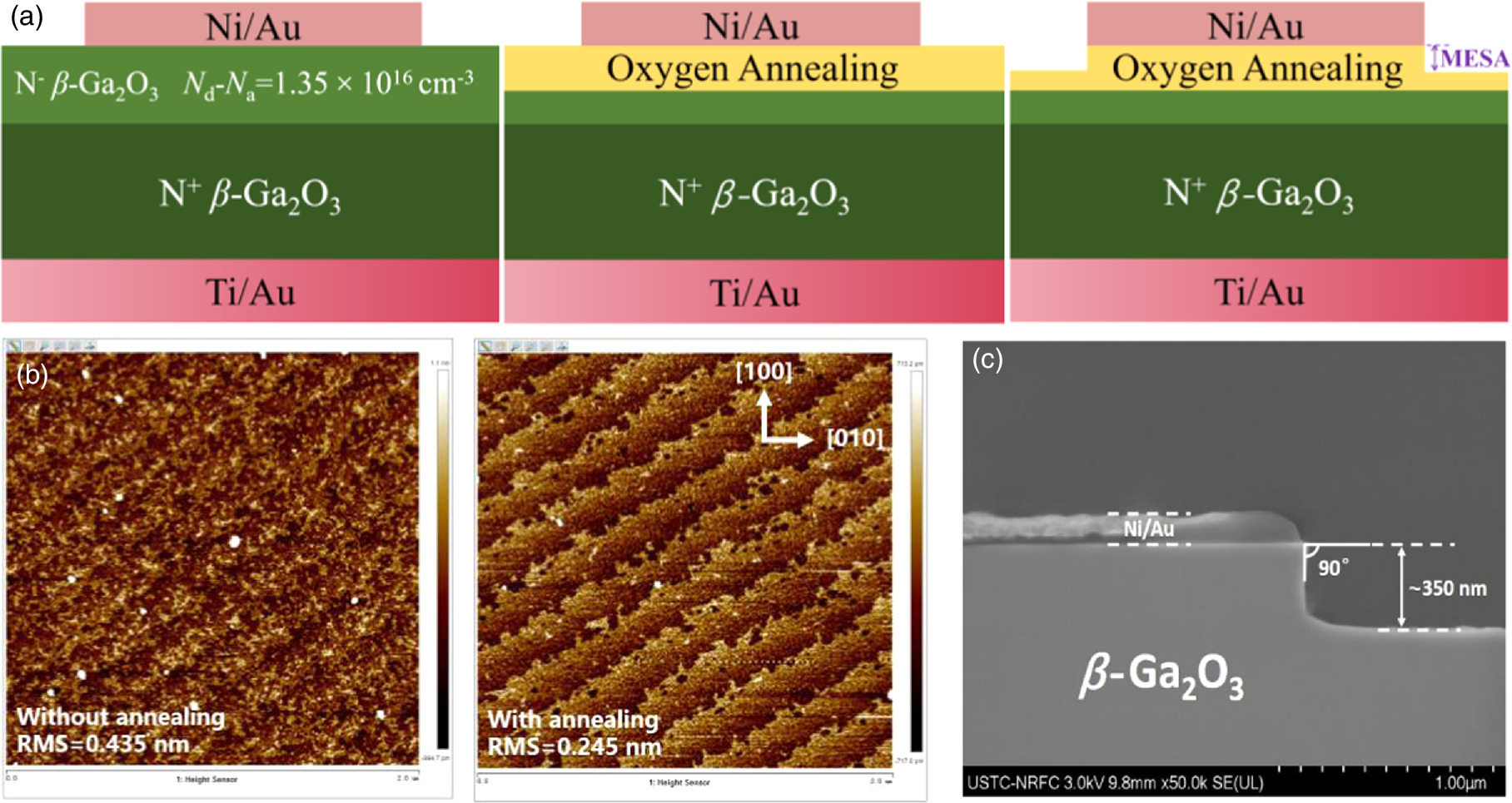
Fig. 1. (a) Schematic cross-sectional view of control β-Ga2O3 SBD (left) and SBD with OA (middle) and SBD with 350 nm mesa termination after annealing (right). (b) The AFM images of the β-Ga2O3 (001) surface with and without surface pre-treatment by OA at 400 °C for 30 min. (c) Cross-sectional SEM of device structure.
Download figure:
Standard image High-resolution imageThe Atomic Force Microscope (AFM) images of the epitaxial layer before and after OA at 400 °C for 30 min are presented in Fig. 1(b). The RMS decreases from 0.435 nm to 0.245 nm in a 2 × 2 μm2 area after annealing and has clear atomic step. Figure 1(c) displays the scanning electron microscopy (SEM) cross-section imaging of the SAMT device with OA, which has an etching depth of approximately 350 nm and an etching angle of 90°.
Figure 2(a) displays the carrier concentration (Nd-Na) extracted by capacitance-voltage (C-V) measurements of devices before and after annealing with different temperatures at 100 kHz. Equation (1) expresses the relationship between the measured capacitance and the Nd-Na of the epitaxial layer.

where q, 
 A is the electron charge, the relative dielectric constant, the vacuum dielectric constant and the anode area, respectively. Annealing caused retraction of the Nd-Na profile approximately 20 nm deeper into the epi-layer and a decrease from 1.35 × 1016 cm−3 to 1.22 × 1016 cm−3 indicating compensation of the surface charge.
8) Figure 2(b) shows the linear plot of the forward I-V characteristics and the extracted differential specific on-resistance (Ron,sp) after annealing at different temperatures. OA caused the current density at 2 V to decrease from 234 A cm−2 (4.12 mΩ·cm2) to 200 A cm−2 (4.62 mΩ·cm2), 196 A cm−2 (4.89 mΩ·cm2), 183 A cm−2 (4.93 mΩ·cm2) and 191 A cm−2 (4.71 mΩ·cm2) at annealing temperature of 200 °C, 400 °C, 600 °C and 800 °C, respectively. This is related to the decrease in carrier concentration after annealing.
9) Moreover, the turn-on voltage (Von) increased after OA of the device. It is due to the increase of the Schottky barrier height, which increased from 1.06 eV (control) to 1.07 eV, 1.08 eV, 1.16 eV, 1.14 eV, respectively. The Schottky barrier height was measured according to Eq. (2):
A is the electron charge, the relative dielectric constant, the vacuum dielectric constant and the anode area, respectively. Annealing caused retraction of the Nd-Na profile approximately 20 nm deeper into the epi-layer and a decrease from 1.35 × 1016 cm−3 to 1.22 × 1016 cm−3 indicating compensation of the surface charge.
8) Figure 2(b) shows the linear plot of the forward I-V characteristics and the extracted differential specific on-resistance (Ron,sp) after annealing at different temperatures. OA caused the current density at 2 V to decrease from 234 A cm−2 (4.12 mΩ·cm2) to 200 A cm−2 (4.62 mΩ·cm2), 196 A cm−2 (4.89 mΩ·cm2), 183 A cm−2 (4.93 mΩ·cm2) and 191 A cm−2 (4.71 mΩ·cm2) at annealing temperature of 200 °C, 400 °C, 600 °C and 800 °C, respectively. This is related to the decrease in carrier concentration after annealing.
9) Moreover, the turn-on voltage (Von) increased after OA of the device. It is due to the increase of the Schottky barrier height, which increased from 1.06 eV (control) to 1.07 eV, 1.08 eV, 1.16 eV, 1.14 eV, respectively. The Schottky barrier height was measured according to Eq. (2):

where q, Js, A*, k, T is the electron charge, the saturation current, the effective Richardson's constant (A* for Ga2O3 to be 41.1 A·cm−2·K−2), the Boltzmann's constant, and the temperature, respectively. Figure 2(c) presents the log-scale measured reverse J-V curves of different devices at 200 V. It can be seen that the reverse leakage density decreases from at least 10−5 A cm−2 to 10−7 A cm−2 after annealing.
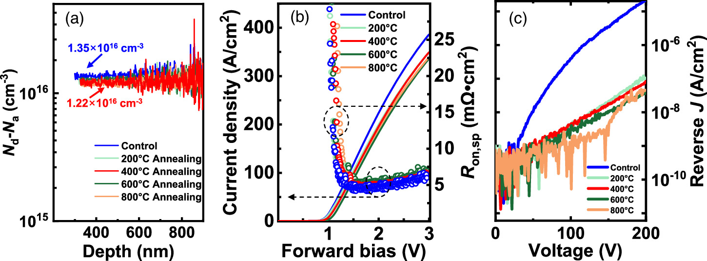
Fig. 2. (a) Nd-Na profile extracted from the C-V characteristics and (b) linear plot of forward I-V characteristics and (c) the reverse leakage density profiles of devices without and with annealing of different OA temperatures at 200 °C, 400 °C, 600 °C and 800 °C (radius of 100 μm).
Download figure:
Standard image High-resolution imageFigure 3(a) shows the statistical plots of the Ron,sp extracted from forward current density and the Vbr of devices with and without OA. As the annealing temperature increased, the Ron,sp increased further, but there is a tendency to saturate after the temperature reaches 400 °C. Meanwhile, the Vbr reached the highest at 400 °C. The highest Power Figure of Merit (PFOM) values without and with different annealing temperatures are 87 MW cm−2 (control), 105 MW cm−2, 173 MW cm−2, 109 MW cm−2 and 112 MW cm−2 at annealing temperature of 200 °C, 400 °C, 600 °C and 800 °C, respectively. Therefore, 400 °C is the optimum annealing temperature for β-Ga2O3 SBDs. It is worth mentioning that the device uniformity of both the Ron,sp and breakdown voltage has been significantly improved after OA.

Fig. 3. Statistical plots of (a) Ron,sp and (b) Vbr for the β-Ga2O3 SBDs without and with OA at 200 °C, 400 °C, 600 °C and 800 °C.
Download figure:
Standard image High-resolution imageThe reverse breakdown I-V characteristics with different annealing temperatures are shown in Fig. 4. The Vbr values are 572 V for the control SBDs and 711 V, 845 V, 691 V and 744 V in ascending order of annealing temperature without mesa termination [Fig. 4(a)]. After 350 nm etching, the Vbr increased to 894 V, 1434 V, 1532 V, 1560 V and 1524 V, which demonstrated the superior performance of the mesa termination [Fig. 4(b)]. It is worth mentioning that the device with OA has a higher Vbr improvement, which can be explained by the repair effect of OA on surface defects and the reduction of reverse leakage current in the HVPE layer.

Fig. 4. The Vbr of the SBDs (a) without and (b) with mesa termination comparison before and after OA at 200 °C, 400 °C, 600 °C and 800 °C.
Download figure:
Standard image High-resolution imageFigure 5 shows the typical optical micrographs of the (001) β-Ga2O3 samples without and with annealing at 400 °C after chemical etching by Potassium hydroxide (KOH) at 80 °C for 1 h. 10) The test samples were obtained from the same one sample (5 × 7.5 mm2). It was divided into two parts of 2.5 × 7.5 mm2 in size. Three 1 × 2 mm2 areas were selected at equal intervals from top to bottom to observe the density of etch pits for each sample. The density without annealing varied from 6700 cm−2 to 2850 cm−2 and 2700 cm−2, but decreased to 6300 cm−2, 900 cm−2 and 1300 cm−2 after OA at 400 °C for 30 min respectively. Besides this, the length and depth of the etch pits were significantly reduced. The reduced pit density on the sample surface helped to reduce the reverse leakage because the electric field tends to concentrate at the bottom of the etch pits, thus minimizing the reverse leakage of the device. 11) The reduction in the pit density and size due to OA may be attributed to the capacity of oxygen groups in an oxygen atmosphere to expedite the adsorption or desorption of surface atoms, thus facilitating surface reconstruction. 12) This can correspond to the AFM results in Fig. 1(b). We also prepared samples annealed in an Ar atmosphere at 400 °C for comparison. However, the density of etch pits did not decrease, indicating that oxygen is necessary to reduce the density of etch pits for β-Ga2O3.

Fig. 5. (a) Optical micrographs of (001) β-Ga2O3 substrate surface after chemical etching by KOH (a) without and (b) with OA at 400 °C for 30 min. Annealing has the obvious effect on reducing the density and the size of the etch pits.
Download figure:
Standard image High-resolution imageFigure 6 presents the I-V characteristics before and after the etching of devices at different annealing temperatures. After 350 nm of etching, the forward current density decreases slightly by 3.8 A cm−2, 1.9 A cm−2, 9.3 A cm−2, and 1.9 A cm−2 at 2 V with annealing at different temperatures from 200 °C to 800 °C. The difference may be caused by the negative interface charges induced by etching and the decrease in the spreading current. 13) The forward turn-on voltage also decreases after that because of the reduction of the interface state which is influenced by the temperature introduced during the in situ annealing dry etching process. 6)

Fig. 6. The I-V characteristics before and after etching of devices with different annealing temperatures of (a) 200 °C, (b) 400 °C, (c) 600 °C, (d) 800 °C (radius of 100 μm).
Download figure:
Standard image High-resolution imageAccording to the above results, the OA treatment at 400 °C is the optimum annealing temperature for β-Ga2O3 SBDs, therefore 400 °C is adopted as the annealing temperature for large area device fabrication. We specially prepared devices via the same fabrication process to verify the feasibility of large current β-Ga2O3 diodes with this design. We achieved a high performance large area device with a Schottky anode area of 3 × 3 mm2. After thickening the device anode electrode, we used a TO-254 shell for packaging as shown in the inset in Fig. 7. The cathode was soldered on the shell, and the anode was connected to the pin though multiple aluminum wire bonding. After that, a parallel sealing and welding process was used to seal the chip in the shell in a nitrogen environment and inert gas was used for protection. As shown in Fig. 7(a), The Von and the Ron are 0.75 V and 121 mΩ, respectively and a forward current of 8.7 A @ 2 V. The breakdown voltage of the SBD is more than 700 V because of the combination of OA and SAMT, as shown in Fig. 7(b).

Fig. 7. (a) Forward conduction characteristics and (b) reverse breakdown characteristics of the 3 × 3 mm2 after encapsulating in the TO-254 package. Inset in (b): packaged device photograph.
Download figure:
Standard image High-resolution imageSeveral reported state-of-the-art β-Ga2O3 devices with approximate sizes (area ≥ 0.8 mm2) are also summarized. Figure 8 shows the benchmark of large area devices between SBDs, PN diodes and Junction Barrier Schottky Diode (JBSD) diodes in the plot of forward current (@2 V) versus breakdown voltage. 5,14–25) Compared with the other devices, our device is at the forefront of the reported work with a PFOM of 45 MW cm−2. For a higher forward current in devices, advanced double-sided packaging and substrate thinning methods are research directions that need to be considered later, as demonstrated by the results reported by Xiao. 18)

Fig. 8. The current (@2 V) versus BV benchmark with the state-of-the-art large area β-Ga2O3 SBDs, Heterojunction Diode (HJDs), and JBSD with close sizes (area ≥ 0.8 mm2).
Download figure:
Standard image High-resolution image
In summary, we successfully developed high performance β-Ga2O3 SBDs by combining the surface pre-treatment method of OA with mesa termination. The characterization results of the devices demonstrate that OA can effectively reduce the surface roughness, and the density and the size of etch pits on the epitaxial layer. It leads to a decrease in the electric field at the pit bottom, resulting in a lower device leakage current and a higher breakdown voltage. Based on this approach, a large area device (3 × 3 mm2) with a forward current of 8.7 A@2 V and a breakdown voltage > 700 V was simultaneously prepared, further confirming the feasibility of this structure in actual high power applications. Moreover, this solution has obvious cost advantages compared with the reported devices with complex terminal structures, making it one of the solutions for commercial β-Ga2O3 SBD production.
Acknowledgments
This work was supported by the National Natural Science Foundation of China under Grant Nos. 61925110, U23A20358 and 62234007, the University of Science and Technology of China (USTC) Research Funds of the Double First-Class Initiative under Grant No. YD2100002009 and YD2100002010, the Collaborative Innovation Program of Hefei Science Center, Chinese Academy of Sciences (CAS) under Grant No. 2022HSC-CIP024, the JieBang Headed Project of Changsha City Hunan Province under grant No. kq2301006, and the Opening Project of and the Key Laboratory of Nanodevices and Applications in Suzhou Institute of Nano-Tech and Nano-Bionics of CAS. This work was partially carried out at the Center for Micro and Nanoscale Research and Fabrication, and the Information Science Laboratory Center of USTC.