
Abstract
Density functional theory was used to investigate the geometric structure of bilayer graphene under an external electric field with carrier doping. Our calculations revealed the crucial impact of external electric fields and the hole injection on determining the geometric structure of bilayer graphene. The bond length of graphene monotonically increased when increasing the hole doping concentration, while it remained insensitive to electron doping. Additionally, there accumulated carriers predominantly distributed in the outermost layer located just below the gate electrode. These results enabled the construction of moiré superlattices in the bilayer graphene, possessing different moiré periodicity depending on the carrier concentration.
Export citation and abstract BibTeX RIS

Content from this work may be used under the terms of the Creative Commons Attribution 4.0 license. Any further distribution of this work must maintain attribution to the author(s) and the title of the work, journal citation and DOI.
Graphene and its thin films have attracted attention in the field of pure and applied sciences due to their extraordinary physical properties and versatile applications. 1–4) In the field of low-dimensional science, graphene stands out due to its exceptional conductivity, mechanical strength, and flexibility. 5–8) These physical properties appear from its unique honeycomb covalent network of carbon atoms, where three of the four valence electrons form strong chemical bonds between C atoms, and the remaining one forms a conical dispersion band around the Fermi level that itinerates through the covalent network. 9–11) Featuring a planar network with fully saturated surfaces, graphene serves as an ideal building block for creating van der Waals complexes through stacking with other graphene layers or two-dimensional materials like hexagonal boron nitride and transitional metal dichalcogenides. 12,13) The electronic structure of these thin films is notably influenced by both the stacking arrangement and constituent layers. 14) Bilayer graphene with Bernal stacking possesses pairs of parabolic dispersion bands at the Fermi level, instead of the conical bands of an isolated graphene. 14,15) Furthermore, a twisted bilayer graphene with a magic angle is a superconductor or Mott insulator thanks to the flat dispersion band at the Fermi level. 16,17) In addition to the thin film structures, the impact of the field effect on the electronic properties of graphene thin films and other van der Waals heterostructures is important in their practical applications. Specifically, a perpendicular electric field transforms bilayer graphene with Bernal stacking and graphene thin films with rhombohedral stacking into semiconductors with a band gap depending on the field strength. 18–22) These facts make graphene and its thin films constituent materials for electronic, energy, and optoelectronic devices.
Although the electronic properties of graphene thin films under the electric field have been well elucidated by various experimental and theoretical works, 5,18–24) the geometric properties of graphene and graphene thin films under the electric field or excess carriers are currently uncertain. The structural information of graphene thin films under the field is also highly demanded for their device applications in terms of their structural stability. Therefore, it is important to know the geometric structures of graphene and its thin films under the external electric field or excess carriers by using the density functional theory (DFT) with an effective screening medium method. Our calculations reveal that the hole carriers elongate the covalent bonds of bilayer graphene. Furthermore, the injected holes show asymmetric distribution between layers. Due to this structural modulation and asymmetric carrier distribution, bilayer graphene can form a moiré superlattice whose moiré periodicity is continuously controllable by tuning the doping concentrations.
All computations were carried out using the DFT 25,26) implemented in the STATE package. 27,28) The generalized gradient approximation with the Perdew–Burke–Ernzerhof functional was utilized to express the exchange-correlation potential energy of interacting electrons. 29,30) The weak dispersive interaction between graphene layers was treated using the vdW-DF2 with a C09 exchange-correlation functional. 31,32) For calculation of the moiré structure, the exchange-correlation potential energy was treated by the local density approximation with a Perdew–Zunger functional to reduce the computational cost because these systems contain over a thousand C atoms. 33) The interaction between valence electrons and nuclei was characterized using an ultrasoft pseudopotential generated by the Vanderbilt scheme. 34) The valence wave function and deficit charge density were expanded using a plane wave basis set with cut off energies of 25 and 225 Ry, respectively.
Field effects on bilayer graphene under DFT are treated by using the effective screening medium method with a structural model of a single-gate FET where the electrode is separated by 5 Å vacuum spacing from the bilayer graphene [Fig. 1].
35,36) The electrode is simulated using an effective screening medium with infinite relative permittivity. Consequently, electrons and holes are introduced into the monolayer or bilayer graphene by injecting the counter holes and electrons into the electrode. The atomic structures were fully optimized until the force acting on each atom was less than  hartree/bohr. Integration over the Brillouin zone was carried out using an equidistant mesh of
  k
points.
k
points.
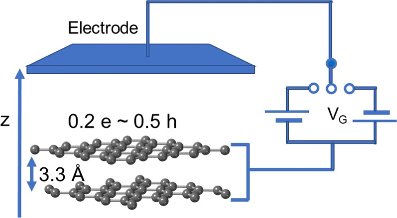
Fig. 1. A structural model of the bilayer graphene field effect transistor. The gray balls indicate the C atoms, and the blue plate indicates the electrode which is connected to a gate power source VG.
Download figure:
Standard image High-resolution imageAn optimized bond length of monolayer graphene under carrier doping is shown in Fig. 2(a). We demonstrated that the bond length of monolayer graphene is extremely sensitive to hole doping. The bond length increases monotonically as the hole density increases. The bond length elongates up to 1.51 Å under the hole concentration of 0.5 holes per unit cell. In contrast, the bond length is insensitive to the electron doping. The bond length approximately retains that under the neutral condition up to an electron concentration of 0.2 electrons per unit cell. Thus, the structural modulation by the excess carriers is asymmetric with respect to the carrier species. This asymmetric structural modulation is ascribed to the band filling of valence and conduction states of graphene. For the hole doping, injected holes are accommodated in the bonding π state, leading to a monotonic downward shift of the Fermi level [Fig. 2(b)]. Thus, the electron density of the covalent bond decreases by the hole injection, resulting in a bond elongation in terms of the hole concentration. For the electron doping, in contrast, the substantial Fermi level shift is absent, even though the electronic structure is highly modulated [Fig. 2(c)]. The Fermi level crosses both the antibonding π state vicinity of the K point and a parabolic band around the Γ point. This fact indicates that the injected electron is mainly accommodated in the parabolic band associated with the nearly free electron states those distributed in the vacuum spacing between the graphene and the electrode. 11) Thus, the electron injection does not affect the charge density of the covalent bonds, leading to insensitivity to the electron doping. Note that the extremely high electron doping may elongate the covalent bond because the electron is accommodated in an antibonding π state.
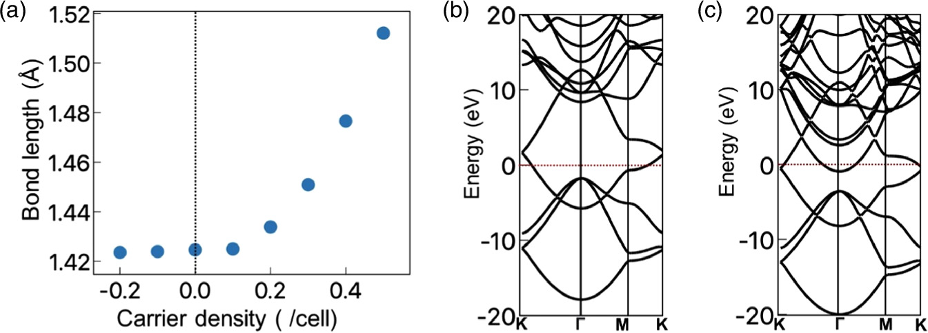
Fig. 2. (a) A bond length of monolayer graphene as a function of carrier species and concentration. A vertical dotted line indicates the neutral position. Electronic structures of monolayer graphene under (b) 0.2 holes per unit cell and (c) 0.2 electrons per unit cell. Energies are measured from the Fermi level energy.
Download figure:
Standard image High-resolution imageWe explored the accumulated charge distribution Δρ(z) of the bilayer graphene across the layers with respect to hole concentration. The polarized charge densities are evaluated by
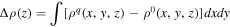
where ρq(x,y,z) and ρ0(x,y,z) are the charge densities with and without excess holes, respectively. The hole concentrations in the top and bottom layers are summarized in Table I, by integrating the polarized charge density  on each layer. Regardless of whether it is stacked in AA or AB arrangements, around 97% of holes are distributed in the layer situated at the electrode side, while 2%–3% of the holes are in the vacuum side layer under a hole concentration of 0.5 holes per unit cell. By comparison, the top layer contains 84%–90% of the injected holes, with hole concentrations of 0.1 and 0.05 holes per unit cell. These results are clear evidence that a significant portion of accumulated holes are located on the topmost layer, regardless of the hole concentrations. In contrast, only a negligible portion of holes are distributed on the bottom layer. This asymmetric carrier distribution indicates that the injected holes have a strong interaction with the negative carriers on the counter electrode so that the top layer feels a strong attractive interaction with the electrode, resulting in the increase of interlayer spacing.
Table I. Carrier distribution ratio on the top and bottom layers of bilayer graphene with AA and AB stacking arrangements under hole doping.
| hole/unit cell | AA % | AB % | ||
|---|---|---|---|---|
| Top | Bottom | Top | Bottom | |
| 0.5 | 98 | 2 | 97 | 3 |
| 0.1 | 89 | 11 | 90 | 10 |
| 0.05 | 84 | 16 | 85 | 15 |
Subsequently, we investigated the electrostatic potential across the layers under the hole doping [Fig. 3]. Under the high hole concentration, the potential mainly drops between the topmost layer and the electrode, because the accumulation of holes mostly occurs in the topmost layer. So, the electric field by the gate electrode is mostly distributed between the topmost layer and the electrode, irrespective of the interlayer stacking arrangement. In contrast, reflecting the carrier penetration to the second layer under the low hole concentration, we found the small potential gradient between the layers, in addition to the primary potential gradient between the topmost layer and the electrode.
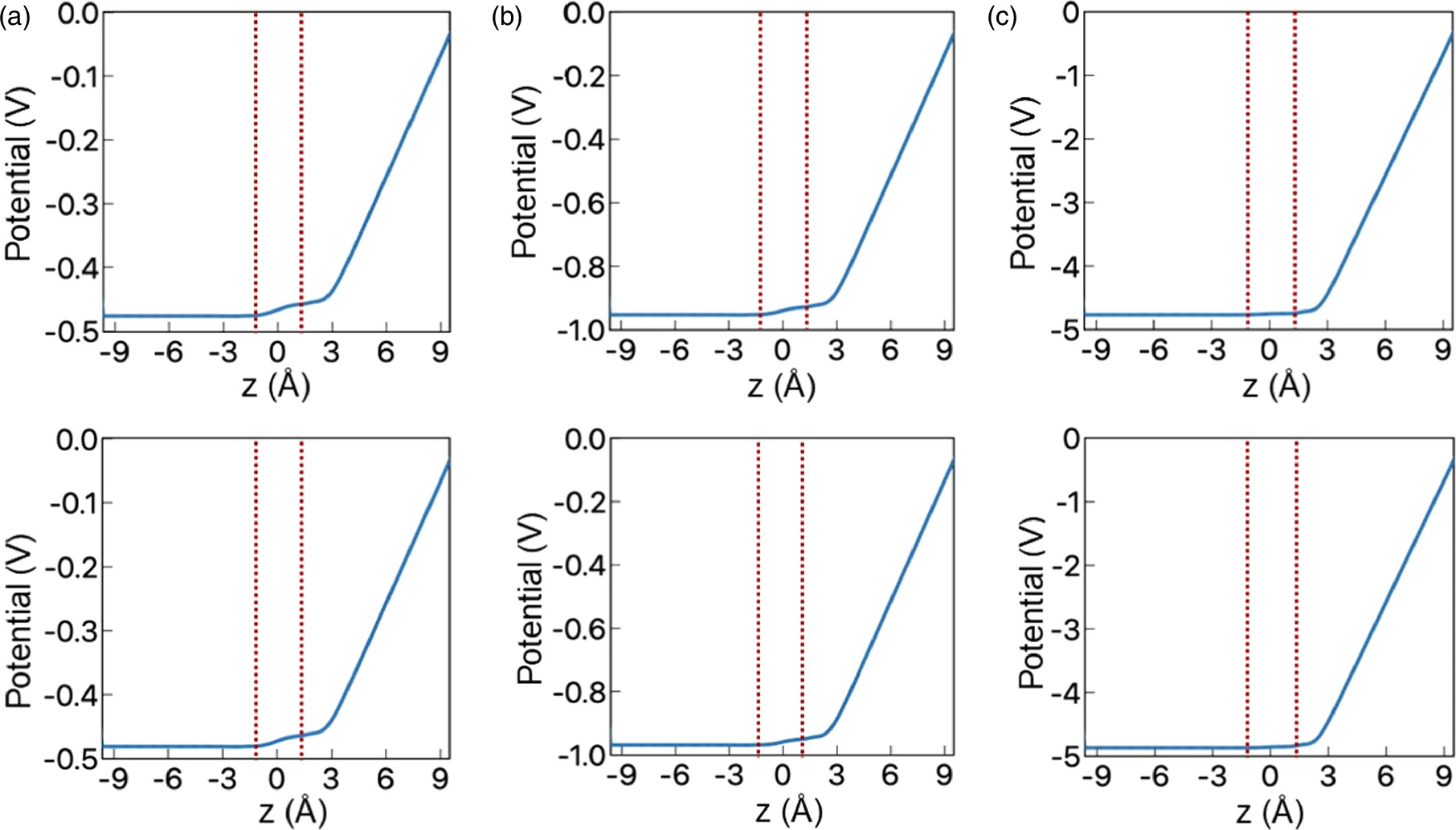
Fig. 3. Electrostatic potential normal to the bilayer graphene with AA stacking arrangements on the top layer and AB stacking arrangements on the bottom layer under hole concentrations of (a) 0.5 holes per unit cell, (b) 0.1 holes per unit cell, and (c) 0.05 holes per unit cell. Red dotted vertical lines denote the position of graphene layers.
Download figure:
Standard image High-resolution imageBy combining the bond elongation depending on the hole concentration with the asymmetric carrier accumulation in the bilayer graphene, bilayer graphene can possess moiré structures whose periodicity depends on the hole concentrations. Here, we consider a moiré structure of bilayer graphene which consists of graphene layers with  and
and  supercells [Fig. 4(a)]. The lattice parameter of the graphene layer with
  supercell is elongated by 5% which corresponds with the 0.4-hole doping per
  unit cell. Under the optimized structures, we found uniform bond lengths in each graphene layer. The length is 1.50 Å and 1.42 Å for graphene layers with
  and
and  supercells, respectively. Furthermore, the height dispersion is also negligible, indicating that the layers retain their flat conformation. In this bilayer graphene, we found the moiré structures reflecting the three representative interlayer stacking arrangements: AA, AB, and BA stacking. Because of the
  and
and  lateral periodicities of the top and bottom layers, the bilayer graphene possesses two different Dirac cones at the K and Γ points corresponding with the top (
 supercell) and bottom (
 supercell) layers, respectively [Fig. 4(b)]. Furthermore, the atomic density difference causes a shift of Dirac point energy between the layers: The Dirac point of the top layer is at −4.8 eV at the K point and that of the bottom layer is at −4.6 eV at the Γ point.
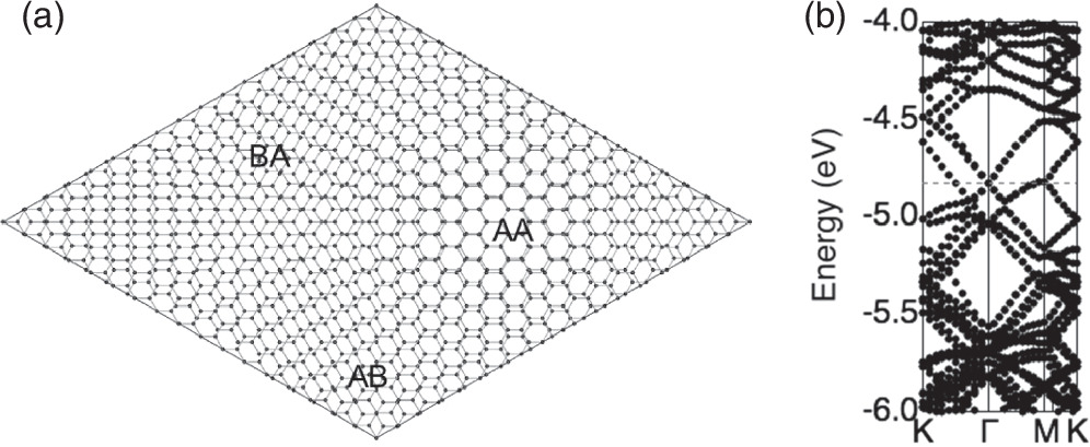
Fig. 4. (a) The geometric structure of bilayer graphene consisting of a  supercell and a
  supercell, where the lattice parameter is elongated by 5%. (b) The electronic structure of the bilayer graphene. Horizontal red dotted lines indicate the Fermi level energy. Energies are measured from the vacuum level.
Download figure:
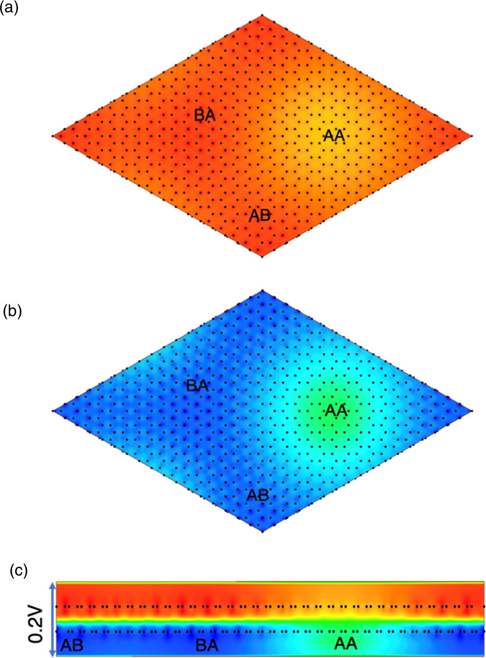
Standard image High-resolution imageFigure 5 shows the electrostatic potential of the top and bottom layers of bilayer graphene. The electrostatic potential showed spatial modulation reflecting the moiré structure. In the top layer where the lattice parameter is elongated by 5%, we found that the potential at the AA stacking region is deeper than those at the AB and BA stacking regions [Fig. 5(a)]. In contrast, for the bottom layer, the potential at the AA stacking region is shallower than those at the AB and BA regions [Fig. 5(b)]. The shallower potential at the AA region is due to the strong hybridization between wavefunctions of the top and bottom layers at the AA stacking region. We also found the electrostatic potential difference of 0.2 V across the layers due to the atomic density difference between the top and bottom layers [Fig. 5(c)]. Note that the moiré periodicity and the potential modulation are continuously tunable by controlling the carrier doping. Moreover, further unique moiré superlattices are expected to occur by applying the external field or hole doping onto the bilayer graphene with twist stacking arrangements.
Fig. 5. The color plot of the electrostatic potential of bilayer graphene consisting of a  supercell and a
  supercell on the (a) top layer (
 supercell) and (b) bottom layer (
 supercell), and (c) the plane across the layers. The red color indicates the higher potential (0.1 V) and blue color indicate the lower potential (−0.1 V) across the layers.
Download figure:
Standard image High-resolution image
In summary, we studied the geometric structure of bilayer graphene under a carrier concentration based on density functional theory with an effective screening medium method. Our analysis revealed that the geometric structure of monolayer or bilayer graphene is sensitive to hole doping, leading to the fact that the lattice parameter monotonically increases when increasing the hole concentration. However, the structural modulation of bilayer graphene is insensitive under electron doping. We also demonstrated that asymmetric carrier distribution occurs between the layers of bilayer graphene under hole doping. Specially with high hole concentration, the accumulated holes are mostly (98%) distributed in the topmost layer in the bilayer graphene just below the electrode. There is no electric field between the layers, and as a result the top layer perfectly screens the electric field. In contrast, when the hole concentration is low, above 80% of holes are distributed on the top layer, while 15%–20% are distributed in the bottom layer. This carrier penetration results in the presence of a finite electric field between the graphene layers. Based on the structural modification and asymmetric hole distribution of the bilayer graphene under carrier doping, the bilayer graphene forms the moiré superlattices by hole doping, whose lattice parameters are continuously tunable by controlling the hole concentration. We demonstrated the moiré structure in bilayer graphene comprising a  supercell and a
  supercell where the lattice parameter is elongated by 5% corresponding to 0.4-hole doping per
  unit. In this bilayer graphene, we observed that the moiré potential induced by the interlayer atomic arrangement. We also demonstrate the two Dirac points at the Γ and K point corresponding to the bottom and top graphene layers, respectively, owing to their different folding conditions on the Brillouin zone.
Acknowledgments
The authors are grateful to the Japan Science and Technology Agency under JST-CREST grant no. JPMJCR20B5 and JPMJCR23A4, the Japan Society for the Promotion of Science under JSPS KAKENHI grant no. JP23H05469, JP22H00283, JP21H05232, JP21H05233, JP21K14484, and JP20H05664, and the Joint Research Program on Zero-Emission Energy Research, Institute of Advanced Energy, Kyoto University. The part of the calculations was performed on an NEC SX-Aurora TSUBASA at the Cybermedia Center at Osaka University.