
Abstract
High-quality and low-defect-density germanium (Ge) buffer layers on silicon (Si) substrates have long been developed for group IV and III–V devices by suppressing defect propagation during epitaxial growth. This is a crucial step for the development of highly efficient photonic devices on Si substrates. Patterned silicon substrates have increasingly been employed for their ability to restrict and hinder the motion of defects. In this work, we demonstrate the effectiveness of an optimised two-step growth recipe structure on a (111)-faceted V-groove silicon substrate with a 350 nm flat ridge. This strategy successfully reduces the threading dislocation (TD) density while growing a 1 μm Ge buffer layer via molecular beam epitaxy. As a result, a high-quality buffer is produced with a low TD density on the order of 107 cm−2 and a surface roughness below 1 nm.
Export citation and abstract BibTeX RIS

Original content from this work may be used under the terms of the Creative Commons Attribution 4.0 license. Any further distribution of this work must maintain attribution to the author(s) and the title of the work, journal citation and DOI.
1. Introduction
Silicon photonics has for a long time attracted a substantial amount of attention due to its versatility, large optical transparency, low cost, and compatibility with complementary metal-oxide-semiconductor technologies for large-area mass production [1–3]. The heteroepitaxial growth of germanium-on-silicon (Ge/Si) is able to serve as a virtual substrate for further epitaxial growth of group IV and III–V active and passive photonic devices for silicon photonics. Indeed, GeSn-, SiGeSn- and GaAs-based photodetector, laser and modulator structures often use Ge as a buffer layer or virtual substrate for integration onto a Si-based platform [4–6]. Despite the promising achievements, the lattice mismatch of 4.2% between Ge and Si results in a significant formation of defects, which are known to damage device performance and degrade lifetime as they penetrate through the epitaxial layers [7, 8]. The dissimilarity of lattice constants leads to a build-up of strain at the interface as the Ge atoms seek to adopt the atomic spacing of Si. When the epitaxial layer exceeds a critical thickness, misfit dislocations form at the heterointerface during epitaxial growth to accommodate the strain and further relaxation is provided by 'threading dislocations' (TDs) which travel up towards the surface [9].
A variety of techniques have been explored over the years to address this issue. Using an array of dopants, such as phosphorous [10], arsenic [11], boron [12], and antimony [13], a reduction of the TD density (TDD) and an improved surface roughness have been observed. Particular attention can be paid to Sb's ability to enhance TD motion and serve as a surfactant, which has enabled a low TDD of  cm−2 for a 500 nm grown Ge/Si sample [14]. Enhanced crystal quality via doping has been vital in reducing the deleterious effects of TDs but with this comes a need to optimise doping densities to prevent dopant segregation from the crystal lattice [15]. Gex
Si1−x
graded buffer layers have also been employed to mediate between the Ge and Si lattice constants to suppress the formation of defects [16–18]. Promising results have been produced from this technique with TDDs on the order of 106 cm−2 but extremely thick buffer layers have been required totalling several microns [19]. Rapid high-temperature (HT) cyclic annealing has proved to be beneficial in supplying thermal strain which enhances the glide of TDs, thereby increasing the chances of them intersecting and self-annihilating [20–22]. In addition, by employing the aspect ratio trapping (ART) technique for selective area growth (SAG), the motion of TDs can be trapped within dielectric silicon oxide (SiO2) walls [23–26]. The high-quality structures achieved from SAG are of great benefit to high-performance devices but as a mask is required during the epitaxial procedure, additional complexity is added to the growth, which can make it difficult to achieve a high yield.
cm−2 for a 500 nm grown Ge/Si sample [14]. Enhanced crystal quality via doping has been vital in reducing the deleterious effects of TDs but with this comes a need to optimise doping densities to prevent dopant segregation from the crystal lattice [15]. Gex
Si1−x
graded buffer layers have also been employed to mediate between the Ge and Si lattice constants to suppress the formation of defects [16–18]. Promising results have been produced from this technique with TDDs on the order of 106 cm−2 but extremely thick buffer layers have been required totalling several microns [19]. Rapid high-temperature (HT) cyclic annealing has proved to be beneficial in supplying thermal strain which enhances the glide of TDs, thereby increasing the chances of them intersecting and self-annihilating [20–22]. In addition, by employing the aspect ratio trapping (ART) technique for selective area growth (SAG), the motion of TDs can be trapped within dielectric silicon oxide (SiO2) walls [23–26]. The high-quality structures achieved from SAG are of great benefit to high-performance devices but as a mask is required during the epitaxial procedure, additional complexity is added to the growth, which can make it difficult to achieve a high yield.
In the past few years, an increasing number of results have shown the effectiveness of using patterned substrates for defect reduction utilising ART. But until recently, Ge growth onto such surfaces had rarely been demonstrated. Amin et al [27] performed rectangular patterning of a Si substrate in order to grow a high-quality 1 μm Ge buffer using chemical vapour deposition (CVD), achieving a low TDD of  cm−2 counted using the etch-pit density (EPD) method. Their research demonstrated defect reduction by restricting the motion of dislocations via faceted sidewalls and consequently showed improved crystal quality for growth on a patterned Si substrate compared with the same growth on a planar Si substrate. 'V-groove' patterned substrates, widely employed for III–V on Si heteroepitaxy, play a crucial role in reducing the density of both planar and line defects. These substrates exhibit the ability to hinder the formation of APDs and foster their mutual annihilation, particularly through interactions with (111) facets, whilst also impeding and redirecting the motion of defects leading to a reduction in TDs [28, 29]. In this report, we adopted an optimised two-step low-temperature/HT (LT-HT) growth process along with rapid HT cyclic annealing in order to grow the 1 μm Ge buffer layer onto a V-grooved Si substrate by molecular beam epitaxy (MBE). This work demonstrates a high-quality flat Ge film with a low TDD of
  cm−2. The Ge structure consists of a thin low-temperature nucleation layer which precedes a thick HT layer and 5 HT cyclic annealing periods to increase the glide of TDs and encourage further annihilation. This is lastly followed by a HT capping layer in order to improve the surface quality.
2. Experiment
The V-grooved Si substrates were fabricated on a standard 8-inch on-axis Si (100) wafer. A 100 nm SiO2 layer was first deposited as a hard mask via plasma-enhanced CVD. Subsequently, 5 grating patterns with different dimensions were transferred onto the SiO2-coated wafer using deep ultraviolet lithography with lengths of 12 mm, a duty cycle of 0.5, and opening widths of 350, 500, 650, 800 and 950 nm. As a result of the scanner's aspect-ratio resolution limitations, it was not possible to reduce the pattern gratings below 350 nm, thereby preventing the fabrication of any patterns smaller than that size. All the gratings are aligned along the [110] direction. Afterwards, fluorine-based inductively coupled plasma dry etching was conducted using the resist as the mask to etch through the SiO2 layer, followed by removing the photoresist in a plasma Asher. The V-grooved Si was finally obtained by wet etching in 25% tetramethylammonium hydroxide (TMAH) solution at room temperature for 90 min after a 10 s hydrofluoric (HF) (20:1) treatment to remove the native oxide layers. Figure 1(a) shows an SEM image of the V-grooves in a 45-degree tilted view exposing the flat ridges and the facets. The V-shape forms due to the selective etching along (100) and (111) planes, where the latter has a much lower etching rate in TMAH [30]. Therefore, the facets of the V-grooves for the epitaxial growth are (111) oriented and the ridges between the V-shaped grooves are (100) planes. Lastly, the 8-inch wafer was diced into 2.1 cm × 2.1 cm substrates before being transferred to the MBE system.

Figure 1. (a) Tiled SEM view of the V-groove substrate with the 950 nm ridges as an example. Five patterns with different size of openings/ridges are fabricated in total which are each separated by non-patterned Si. (b) Ge buffer schematic.
Download figure:
Standard image High-resolution imageThe growth took place inside of a Veeco Gen 930 solid source MBE. A schematic of the buffer structure is depicted in figure 1(b). The wafer was first precleaned at 600 °C for 1 h to remove contaminants after being exposed to the atmosphere following fabrication. This was followed by a 20 min deoxidation process at a high temperature of 1000 °C in order to remove an ultra-thin thermally erasable surface protecting SiO2 layer, as detailed in Hou et al [31], to ensure a high-quality and reactive surface for the subsequent growth. An initial 50 nm Ge wetting layer was deposited at a LT of 250 °C with a low growth rate of 0.5 Å s−1 to ensure an evenly coated nucleation layer across the substrate. Furthermore, it is necessary to reduce the surface mobility of the Ge atoms and thus restrict 3D island formation, which is made possible by the LT. Subsequently, an 850 nm thick Ge layer was grown at a HT of 650 °C with a high growth rate of 1.5 Å s−1. Conversely, the HT growth increases the diffusion length of the Ge adatoms, which encourages movement into the grooves. Thermal energy is also provided to the TDs, which in turn increases the probability that those which possess opposite Burgers vector signs will meet each other and annihilate. In addition to the HT, employing a significant thickness ensures uniform filling of the grooves and promotes the development of a flat surface for the buffer. Following this, 5 periods of cyclic annealing were performed, each of which lasted for 5 min at temperatures of 950 °C and 650 °C. The rapid switching between high temperatures induces thermal strain which is crucial for encouraging TDs to propagate further along the (111) direction and self-annihilate with one another. To further flatten the surface and improve crystal quality post annealing, a 100 nm HT capping layer at 650 °C was grown with a high growth rate of 1.5 Å s−1.
The defect density is determined using electron channelling contrast imaging (ECCI) and the surface roughness is examined using atomic force microscopy (AFM) operating in tapping mode. Lastly, cross-sectional (scanning) transmission electron microscopy ((S)TEM) lamellae provide more insights into the nature of defects and strain distribution at the Ge/Si interface, down to the atomic scale (see: methods).
3. Results and discussion
Following the growth of a 1 μm Ge buffer layer, ECCI scans are taken to determine the density of TDs. This scanning method relies on electron channelling from the SEM to produce highly contrasted images and serves as a more accurate technique than EPD when measuring the defect density as dislocations can easily be differentiated within the contrast imaging. Whilst only requiring minimal sample preparation, ECCI still possesses the ability to detect strain field changes at the surface enabling high resolution images [32–34]. AFM was performed to determine the surface roughness while STEM was conducted to map defect distribution near and at the heterointerface. Figure 2 illustrates changes in the surface quality from plan-view ECCI scans as a function of the ridge width. Most notably, an array of bright and dark stripes is visible, which is related to both the high contrast and roughness of the images, and it can be seen that the TDs exist mainly along the darker patches. The dark stripes represent places where the buffer surface has slumped and not flattened evenly: the effect is more pronounced as the flat ridge width increases from figures 2(a)−(d). Furthermore, both the 500 nm and 650 nm ridge widths in figures 2(a) and (b) show substantially less TDs compared with the larger dimension sizes in figures 2(c) and (d). From these plan-view SEM images (in channelling geometry), it appears that whilst some defects might potentially be harder to determine due to the roughness, as is most clear in figure 2(d), the contrast in quality remains evident. This is likely due to a relationship between the generation of misfit dislocations and the surface area of the flat ridges [35].
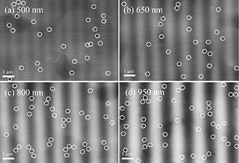
Figure 2. ECCI scans for the 500–950 nm ridge width dimensions after 1 μm Ge growth. The dark stripes where TDs are evident increase in size from (a)–(d) suggesting degradation in crystal quality.
Download figure:
Standard image High-resolution imageFigure 3 demonstrates the general trend of TDD with respect to the strip ridge width, where '0 nm' refers to an unpatterned Si surface. The 950, 800, 650, 500, 350 nm strips and unpatterned Si exhibit TDDs of,  cm−2,
cm−2,  cm−2,
cm−2,  cm−2,
cm−2,  cm−2
cm−2
 cm−2 and
  cm−2 respectively. The high crystal quality achieved for the buffer on a strip width of 350 nm can be seen from the plan-view ECCI scan in figure 4(a) compared to the buffer surface on unpatterned Si in (b) where for both, each TD is circled by a white circle. The results of figure 3 suggest that the existence of a patterned region in and of itself is not sufficient for the reduction of defects, as initially might be thought, but that in fact careful consideration must be given to the shape and geometry of the pattern. Furthermore, the result on the 650 nm strip being superior to the 500 nm strip is unexpected but this was not investigated further as they are both still higher than the TDD on the 350 nm strip. It is worth noting that all the patterns exist on the same substrate and are separated by unpatterned Si, which may influence the growth dynamics for each patterned area. With this assumption, a more precise understanding of a particular dimension's capabilities could be attained in future by using one dimension size per substrate. The low defect density is thought to stem from three contributing factors: (1) the V-groove substrates' ability to trap dislocations in accordance with ART which prevents them from travelling through the buffer layers, (2) the facet angle's ability to redirect TDs ensuring a greater probability of self-annihilation and (3) thermal strain from cyclic annealing which provides the energy necessary for TDs to glide further in the (111) for further mutual annihilation. More specifically, it is also believed that TDs which are not trapped by the sidewall facets can merge with misfits on top of the flat ridges [36]. In the case where the motion of TDs within the groove has already been impeded, misfit dislocations no longer function as 'sinks', which then allows TDs from the flat ridge to propagate upwards and thus explains the higher defect densities for the larger ridge widths. Besides, the observed reduction in TDs is not as substantial as initially anticipated, which is primarily attributed to geometrical changes in the substrate shape as discussed later.
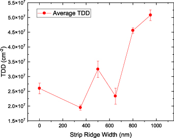
Figure 3. Trend graph for the TDD with respect to the flat ridge width. The '0 nm' strip width refers to the unpatterned planar Si area.
Download figure:
Standard image High-resolution image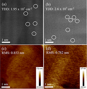
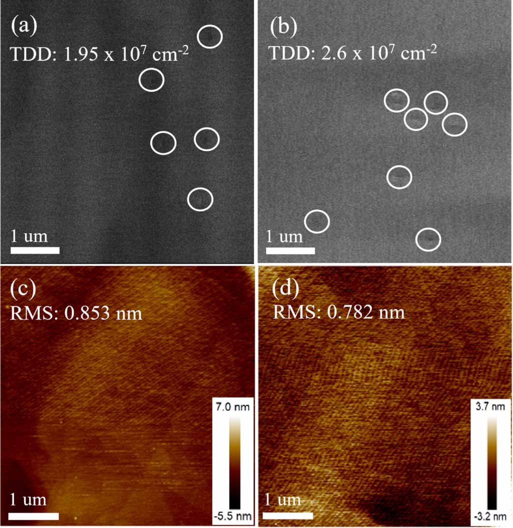
Figure 4. (a) and (b) show ECCI scans for growth on a 350 nm ridge width V-groove and planar Si substrate, respectively. Each TD is circled on top of the Ge surface in both. AFM images show an RMS for Ge on V-groove (c) and also planar Si (d).
Download figure:
Standard image High-resolution imageThe surface morphology of each strip can be visually inspected before further in-depth examination. Following the fabrication of the V-groove patterns, a spectrum of colours can be seen on the substrate due to light reflecting off the silicon facets at different angles. When the grooves are completely filled and the surface is flat, this spectrum can no longer be observed. The surface roughness after 1 μm Ge growth was analysed using AFM, which provides a root-mean-square (RMS) roughness of 0.853 nm and 0.782 nm for the 350 nm strip and planar Si surface, respectively, as shown in figures 4(c) and (d). As mentioned earlier, the buffer thickness plays an important role in achieving a low surface roughness. Due to an uneven substrate surface, it would be particularly challenging to reduce this much further with a thinner structure. Despite the low RMS in figure 4(c), a faint pattern can still be seen on the surface, suggesting that there is room for optimising the growth recipe for the 350 nm strip specifically.
In order to better understand how the growth of Ge on V-groove Si evolves into a flat surface, a two-step 350 nm buffer, including a 50 nm LT Ge wetting layer and a 300 nm HT Ge layer, was grown. The 350 and 650 nm strips are considered here due to having the lowest defect densities. Figures 5(a) and (b) show cross-sectional SEM images of the V-groove buffer after 350 nm of Ge growth for both substrate dimensions. Figure 5(a) shows that whilst the grooves are completely filled after 350 nm buffer deposition, significant roughness can be observed on the undulating surface. In figure 5(b), the wider ridge has led to periodic facets at the Ge buffer surface showing an almost V-groove-shaped Ge surface. Comparing the SEM image of the 350 nm strip in figure 5(a) with the SEM plan view in figure 4(a), it is observed that as the HT growth occurs, the increase in surface mobility has helped to improve the surface flatness. Whilst the high degree of roughness for larger ridge width dimensions is likely to present an issue for further epitaxial growth of group IV materials, it is possible to use LT deposition to further reduce the migration length of the Ge atoms and achieve well-defined facets which lie along the (111) plane or higher planes for III–V on Si integration [37]. In addition, a thinner buffer would only be necessary as the objective shifts from seeking to flatten the structure to achieving a faceted buffer layer. This would solve the issue of APD generation between polar and non-polar materials.
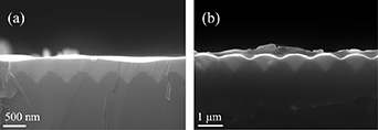
Figure 5. SEM images of 350 and 650 nm strips after 350 nm Ge growth. (a) Cross-section SEM for the 350 nm strip clearly shows an uneven surface. (b) Cross-section SEM for 650 nm strip shows a faceted Ge layer resembling the substrate underneath with flat regions and facets.
Download figure:
Standard image High-resolution imageA better understanding of the buffer quality on the patterned substrate is investigated via high-resolution STEM imaging which provides an insight into the growth quality above the 350 nm Ge strip substrate. A cross-sectional FIB lamella was prepared as seen from the SEM image in figure S1. Figure 6 shows cross-sectional high-angle annular dark field (HAADF) images of the Si/Ge interface. The high-resolution images were acquired along the [011] zone axis (Fourier transform (FFT) inset is included for completeness). Figure 6(a) shows the shape of the grooved Si, and contrary to the conclusion that could be drawn from the lower-magnification view in figure 1(a), it appears that the grooves are not perfectly V-shaped following the growth: a flat region of 230 nm is observed at the peak, which is likely to be a consequence of the HT cyclic annealing. On closer examination, a rough interface is observed between the Si and Ge along the patterned area. This is the case in particular on the flat region after the ridge as highlighted with a blue square in figure 6(a). In contrast, a smoother interface is observed at the faceted ridges (regions highlighted with a yellow and red square in the same figure). Furthermore, defects at the Si/Ge interface, such as dislocations and stacking faults, were also observed (see figure S2). The uneven HAADF contrast across the interface hints at both possible significant interdiffusion of Si and Ge, both along the (111) and (001) flat ridges, as well as pronounced roughness through the sample thickness (along the beam direction), resulting in overlapping regions with both Si and Ge (see figure 6(a) (i)–(iii)). This interface roughness can be attributed to the prolonged period of HT growth as well as the HT cyclic annealing. This is further highlighted by the high-resolution images in figure 6(a) (iv)–(vi), showing the degree of intermixing at the atomic level. Further HAADF images are shown in figure 7 in order to understand the behaviour of defects as they propagate from the patterned substrate. Near the Ge/Si interface, TDs exhibit pronounced bending, promoting self-annihilation and effectively preventing their progression toward the surface (see figures 7(a) and (b)). Moreover, the induced stress during HT annealing plays a pivotal role in the additional bending of these defects which is necessary both inside and outside the trench. Additionally, the facet wall is noted to serve a dual role: the redirection of TDs, through its angled orientation, whilst simultaneously serving as a barrier that impedes their path, as made clear in figure 7(c). Lastly, in figure 7(d), much defect interaction is noted at the corner of the patterned groove where few defects travel further upwards. The concentrated nature of such dislocations increases their probability of colliding and inhibits their threading properties. It is worth noting that the patterned substrate has not prevented the emergence of TDs, the strain accumulated from the lattice mismatch still persists. This underscores the need for an optimised growth structure. Besides, the trench depth requires optimisation to enable more effective trapping of dislocations, particularly as some defects have been able to glide away from the grooves. Further conventional bright-field HRTEM in figure 8 examines the corner of the grooved area from where a higher density of dislocations appears to manifest. Significant propagation of line defects is observed in conjunction with an intermixed interface, further highlighting the shape change of the substrate. As indicated by the black arrows, the increased prevalence of defects heightens the likelihood that TDs meet and mutually annihilate with one another. This helps to ensure a high crystal quality across the surface. The smaller than expected reduction in TDD underscores the imperative for additional optimisation, particularly in fine-tuning the flat ridge width and refining the facet shape. These adjustments are deemed essential to achieve a more pronounced reduction in defect density, ideally reaching the order of 106 cm−2.

Figure 6. HAADF images of the Si/Ge interface in the V-grooved area of the 350 nm ridge width Ge sample at large and small scales. (a) HAADF image showing the V-groove Si/Ge. Inset shows the corresponding FFT where the (111) spots are circled in white. Subsections (i)–(iii) of (a) show high-resolution (HR) HAADF images of the Si/Ge interface at the regions highlighted with coloured squares at a 2 nm scale size. Subsections (iv)–(vi) are further zoomed in HR HAADF images showing the atomic arrangement at the Si/Ge interface as indicated by the black squares in (i)–(iii) for the V-grooved region at a 1 nm scale size.
Download figure:
Standard image High-resolution image
Figure 7. HAADF exhibiting defect behaviour within the V-groove. Figures (a) and (b) shows defects bent towards each other, whereas (c) and (d) show defect blocking from the facets and self-annihilation at the edge of the flat region, respectively.
Download figure:
Standard image High-resolution image
Figure 8. Cross-sectional HRTEM image of Ge/Si interface viewed from the (110) plane. Strain relaxation occurs via intermixing and defect propagation. The black lines highlight line defects, many of which self-annihilate within approximately 40 nm without travelling much further. GPA strain analysis is provided in figure S3 for the enclosed blue square.
Download figure:
Standard image High-resolution image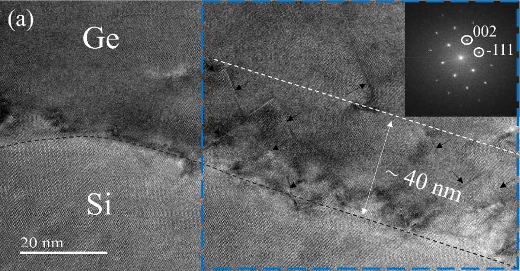
4. Conclusion
A 1 μm Ge buffer film with a low TDD has been grown by MBE using an optimised LT-HT growth technique followed by 5 short periods of cyclic annealing on a (111)-faceted V-groove Si substrate. Five different ridge widths of 350, 500, 650, 800 and 950 nm were fabricated onto a Si substrate. A low RMS of 0.853 nm has been demonstrated largely in part due to the thick HT layer which encourages a uniform growth morphology. Furthermore, a low defect density of  cm−2 shows that an optimised two-step growth onto a V-groove patterned substrate with a current optimal 350 nm ridge width and (111) facets can offer a comparatively low TDD. The use of an on-axis V-groove substrate enables the trapping of TDs by making use of the ART technique. In addition, TD bending has been observed within the grooves, as well as self-annihilation above the substrate from HT cyclic annealing induced stress, which collectively help to ensure a high-quality buffer as evidenced from the plan-view ECCI scan. Using patterned Si substrates can allow for better functionality and the ability to fabricate a variety of complex structures suited for defect reduction, which makes it an exciting domain for the future. These findings highlight the important role of patterned V-groove substrates in facilitating high-quality crystal growth and consequently their widespread applicability for developing optical components with high performance.
5. Methods
A Veeco Gen 930 solid-source MBE fitted with Knudsen effusion cells was used to carry out the Ge growth. Two Ge sources, Ge-1 and Ge-2, present two growth rate options. Ge-1 offers a low growth rate of 0.5 Å s−1, with tip and base temperatures set at 1320 °C and 1260 °C, respectively. Conversely, Ge-2 provides a high growth rate of 1 Å s−1, with tip and base temperatures of 1314.4 °C and 1254.4 °C, respectively. A 3-inch wafer holder with a 4 cm2 wafer adaptor is used to secure the wafer on to the substrate holder. The growth is monitored using in-situ RHEED with an electron gun operating at a voltage of 15 kV with a current of 1.4 A. AFM was performed using a Veeco Dimension 3100 AFM using standard tapping mode operation under ambient conditions using n-doped silicon tips. ECCI measurements were conducted using a Focused Ion Beam Zeiss XB1540 Crossbeam SEM with a 30 μm aperture and an electron high tension of 30 kV. In order to determine the defect density, multiple scans of the different strip widths are performed each covering an area of 77 μm2. Four dislocation density measurements for each strip are taken in order to determine the average TDD and the standard error of the mean is calculated to provide the uncertainty. The data is plotted using OriginPro. FIB Lamellae were prepared in a Hitachi Ethos NX5000 FIB-SEM at the SuperSTEM laboratory. Carbon was deposited by the electron and ion beams on the region of interest prior to the lamellae being lifted out to copper grids and thinned using successively lower currents of 30 kV Ga+ ions to a thickness of a few hundred nm. Smaller areas of interest were further thinned using currents and energies down to 5 kV and 20 pA Ga+. Areas around these windows were kept thicker as a natural frame for stability and heat dissipation. Finally, 1 kV Ar+ polishing was applied to remove remnant damage from low-kV Ga+ milling. Atomically resolved STEM imaging was carried out on a probe corrected Nion UltraSTEM microscope and a Nion UltraSTEM100MC—Hermes at 100 kV. The instruments are equipped with a cold field emission electron source with a nominal energy spread of around 0.3 eV. The microscopes feature an ultra-stable stage, conventional bright field, (0–6.5 mrad) angular range and HAADF (90–190 mrad) angular range imaging detectors. The probe forming optics were adjusted to provide a 1 Å probe with a beam convergence of 30 mrad (half-angle).
Acknowledgments
This work was supported by the UK Engineering and Physical Sciences Research Council (EP/P006973/1, EP/R029075/1, EP/T028475/1, EP/V036327/1, EP/V048732/1, EP/W021080/1, and EP/X015300/1, EP/S024441/1).
Data availability statement
All data that support the findings of this study are included within the article (and any supplementary files).
Supplementary data (1.4 MB PDF)