
Abstract
In this work, degenerate n-type GaN thin films prepared by co-sputtering from a liquid Ga-target were demonstrated and their low-field scattering mechanisms are described. Extremely high donor concentrations above 3 × 1020 cm−3 at low process temperatures (<800 °C) with specific resistivities below 0.5 mΩcm were achieved. The degenerate nature of the sputtered films was verified via temperature-dependent Hall measurements (300–550 K) revealing negligible change in electron mobility and donor concentration. Scattering at ionized impurities was determined to be the major limiting factor with a minor contribution of polar optical-phonon scattering at high temperatures.
Export citation and abstract BibTeX RIS

Content from this work may be used under the terms of the Creative Commons Attribution 4.0 license. Any further distribution of this work must maintain attribution to the author(s) and the title of the work, journal citation and DOI.
The use of GaN-based low-noise and high-power amplifiers and their hetero-integration into conventional Si-CMOS technology are of major interest for next-generation communication systems. 1–3) To meet the increased data rate requirements, higher frequencies with improved efficiency and bandwidth are targeted. 3,4) However, downscaling of the gate length to address higher frequencies requires a significant reduction of parasitic resistances in the devices. 3,5) The access resistance of highly-scaled high-electron-mobility transistors (HEMTs) or multi-channel devices 6) suffers from the inherent metal–semiconductor barrier for high Al-content barriers. 4,7) A current transport mechanism completely determined by tunneling is desirable to achieve the lowest possible voltage drop at the metal–semiconductor interface. Removing the AlGaN-barrier and/or rendering the sub-contact area n-type is the only possibility to change the electron transport across the barrier to the 2-dimension electron gas from a thermionic to field-emission type at higher Al-contents. However, achieving high carrier density (n > 1 × 1020 cm−3) for a field-emission-based current transport is difficult due to the decreasing crystal quality. In addition, low-temperature processes on a large wafer scale are beneficial to protect the AlGaN/GaN interface in a HEMT.
In this work, the transport properties of heavily Si-doped GaN thin films deposited by co-sputtering from Si and from a liquid Ga target and on 4-inch sapphire substrates are investigated. Extremely high carrier concentrations (n > 3 × 1020 cm−3) are demonstrated. Specific resistivities below 0.5 and 3.5 mΩcm are achieved at growth temperatures of 800 °C and 590 °C, respectively. Carrier mobilities were found to be limited by scattering at ionized impurities at high Si doping levels. The donor–acceptor compensation ratio was found to be nearly constant below θ ≈ 0.2 even beyond n > 1 × 1020 cm−3 different from the reported data by metalorganic CVD (MOCVD) and MBE. Temperature-dependent Hall measurements revealed negligible change in carrier density (n) and mobility with increasing temperature indicating Mott-transition from a semiconducting to a metallic character. Carrier densities and specific resistivity at low growth temperatures (≤800 °C) are found well beyond reported data of MOCVD-grown thin films. The results demonstrate the feasibility of sputtered GaN from a liquid Ga target as an alternative process with high n and easy upscaling beyond 4-inch suitable for future process integration into future radio-frequency or optoelectronic (e.g., tunnel junctions) GaN-based devices.
The recent focus of advanced contact processes is generally driven by CMOS-compatible, Au-free, and/or low-temperature budget ohmic contacts, 8–12) or n-GaN regrowth for highly-scaled AlGaN 5) or novel Al(Sc)N-based HEMTs 13–15) with high Al-content. The fabrication of highly n-type doped GaN films was demonstrated via Si implantation, 13,16,17) MBE, 18–21) MOCVD 22–26) (Si or Ge), pulsed laser deposition (PLD) 27) and reactive, pulsed sputtering (PVD) from a solid Ga target. 15,28–31) Si implantation is used for GaN-devices but faces issues to achieve carrier densities and requires a high-temperature treatment to recover for the implantation damage. 16) MBE-regrown layers are commonly applied due to the low growth temperature but face issues in terms of upscaling, throughput, and homogeneity. 20) MOCVD regrowth was demonstrated at low growth temperatures 23) with reduced growth rate, but is limited in terms of achievable n > 5 × 1019 cm−2 at 550 °C and does not offer a non-selective growth mode 24,25) to avoid growth inhomogeneities. 25,32) Typical growth with high growth rates is conducted at higher temperatures (>950 °C). 24,25) Reactive sputtering was demonstrated with high n and high mobility 29,30) on 300–600 nm thick films. However, the used Ga-targets need to be heavily cooled to remain solid during sputtering. 33) In addition, the cooling system gets more complex for larger wafer diameters. Alternatively, ceramic GaN targets can be used but are difficult to handle due to high impurity concentrations. The use of a liquid Ga target avoids the need for a complex cooling system and can be easily filled up while no sputter craters occur during growth. In addition, the liquid target can be easily upscaled to larger wafer diameters and lower parasitic doping occurs when compared to ceramic GaN targets.
Three samples (A–C) were initially grown by MOCVD on sapphire with an Fe-doped buffer topped with a 200 nm unintentionally-doped GaN layer to compensate for Fe segregation. 34) The sheet resistance of samples A, B, and C was measured after MOCVD buffer growth via a contactless eddy current revealing an RS > 100 kΩ/sq. GaN films were deposited by co-sputtering of a Si bar and a liquid Ga target in an Evatec Clusterline® 200II with a modified process module. A detailed description of the basic sputtering setup/process can be found elsewhere. 35) 150 nm Si-doped GaN (± 6%) was sputtered on top of the MOCVD-GaN with nominal growth temperatures of 590, 700, and 800 °C. Sample D was prepared by directly sputtering GaN:Si on sapphire. Si contamination of the target could be present but not quantifiable so far. FWHM were derived from fitting two pseudo-Voigt functions assuming that the peak with lower intensity is related to the sputtered, Si-doped GaN. The FWHM of the MOCVD-grown buffer was found to be FWHM = 0.064°. Fitting the sample with the lowest growth temperature was not possible due to the low side-peak intensity.
Atomic force microscopy was used to determine the rms to reveal the smoothest surface morphology with the lowest growth temperature. A summary of the structural properties is given in Table I.
Table I. Structural properties of co-sputtered n-GaN: tn-GaN—thickness of Si-doped GaN-layer, TH—nom. Heater temperature, GR—growth rate, rms—root mean square, FWHM - full-width half maximum of the 00.2.
| Sample | Substrate | tn-GaN [nm] | TH [°C] | GR [nm s–1] | rms [nm] | FWHM (00.2) [°] | Polarity |
|---|---|---|---|---|---|---|---|
| A | GaN/sapphire | 150 | 700 | 0.9 | 0.58 | 0.188 | Ga |
| B | GaN/sapphire | 150 | 590 | 0.9 | 0.38 | — | Ga |
| C | GaN/sapphire | 150 | 800 | 0.9 | 0.91 | 0.134 | Ga |
| D | Sapphire | 1005 | 800 | 0.6 | 21.6 | 0.437 | N |
The theoretical metal–semiconductor transport properties (thermionic emission - TE, thermionic field emission - TFE; field emission—FE) are dependent on the characteristic energy E00, which in turn is dependent on the n in the sub-contact area as following: 36)

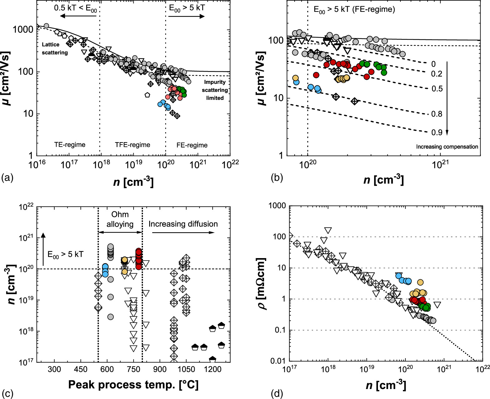
With q, h, εr (9.5), mtun* and m (mtun*/m = 0.22) are the elementary charge, Planck constant, relative dielectric constant, effective tunneling mass, and electron mass, respectively. We use the simple differentiation: 36) FE: E00 ≤ 0.5kT; TFE: 0.5kT ≤ E00 ≤ 5kT and E00 ≥ 5kT. Thus, to achieve E00 ≥ 5kT a donor concentration of n > 1 × 1020 cm−3 is required for GaN. Fundamental low-field transport properties are characterized by Hall measurements at RT. 200 μm Ti-based contacts pads were evaporated via shadow masks and mechanically isolated (1 × 1 mm2 isolation, field = 0.52 T). The use of co-sputtering a Si bar comes along with the possibility of achieving a gradient in Si concentration over the same wafer depending on the distance of the wafer area to the Si bar. Thus, several carrier concentrations and corresponding carrier mobilities can be measured on the same wafer. Carrier densities of n = 6.7 × 10¹⁹ to 3.7 × 1020 cm−3 with carrier mobilities of μ = 21 to 42 cm2 Vs–1 were found over all samples. No Si segregation was observed in the films via transmission-electron microscopy. Improved compensation ratios were found with increasing heater temperature as given in Fig. 1. The achieved carrier densities are well beyond the state-of-the-art reported for MOCVD and MBE at lower growth temperatures [Fig. 1(c)]. The extremely high carrier concentrations would be well suited to address source starvation issues causing linearity distortion in highly-scaled GaN-HEMTs. 37)

Fig. 1. (a) n versus μ reported in the literature for various growth methods: MOCVD (quarters with a cross); MBE (diamonds); HVPE (pentagons) reactive sputtering (grey circles); Si implantation (half-filled hexagons). Samples in this work are colored: sample A (yellow); B (blue); C (red); and D (green). Solid and dotted lines represent fitting from Schwierz et al. based on Caughey–Thomas approximation; 38) (b) n versus μ in the range of E00 > 5kT. (c) Peak process temperature versus measured n. Reported range of alloying temperatures of ohmic contacts to AlGaN/GaN are added; (d) n versus specific resistivity.
Download figure:
Standard image High-resolution imageIn general, several scattering mechanisms could be assumed for the co-sputtered GaN:Si even though impurity scattering is most likely dominating at high donor concentrations. 38) Scattering at ionized impurities in dependence of the compensation ratio θ = ND/NA can be expressed by: 39)

With:

And NI and m*F are the ionized impurity concentration and effective mass at the Fermi energy, which is given by:

with

and:

Where α (0.64) and m* e (0.22me) are the non-parabolic conduction band coefficient [α = 1(m*e/me)]2, and the electron effective mass, respectively. High carrier compensation ratios θ = ND/NA were found for MOCVD and MBE-grown samples beyond n > 1 × 1020 cm−3 as shown in Fig. 1(b). As a consequence, a strong mobility decrease was reported limiting the achievable n and specific resistivity. Compensation ratios of the co-sputtered thin films in this work were found to be rather constant up to n = 3.7 × 1020 cm−3 at higher growth temperatures. A significant increase in compensation ratio is observed at lower growth temperatures (θ = 0.8), which could be attributed to a decrease in crystal quality where e.g., an increasing amount of point defects 40) or an increase in impurity incorporation (e.g., carbon). The assumption is consistent with the increase in FWHM. Specific resistivity was derived and compared to reported data from the literature 18,19,21–24,29,30,41,42) (Fig. 1). Lowest specific resistivities in this work were obtained for highest growth temperature (800 °C) with ρ < 0.5 mΩcm. An increase in resistivity is observed by lowering the growth temperature as a result of the increasing compensation ratio. The lowest resistivity of sample A (590°) was found to be 3.5 mΩcm. To verify Mott transition temperature-dependent Hall measurements were carried out for T = 300–575 K. No significant change in electron concentration or mobility was observed indicating the degenerate nature of the Si-doped GaN. Temperature-dependent polar optical-phonon scattering was modeled via: 43)

where Ћω0 is the optical-phonon energy (100 meV). Scattering at dislocations is neglected since their impact on transverse mobility above n > 1 × 1020 cm−3 for dislocation densities below NDISL < 1 × 1011 cm−2 is not relevant. 44) Dislocation densities of MOCVD-grown GaN on sapphire are generally found to be much lower and the interface of sputtered GaN on MOCVD-GaN is not expected to generate new dislocations. Scattering at grain boundaries could be assumed for sputtered GaN, however, the associated potential barriers would lead to a thermal activation of μ or n. In addition, at high doping levels, most of the grain boundary-related trap states are filled and the potential barriers would decrease in height and width. 45) Temperature-dependent fitting of μ was achieved using Eqs. (2) and (7) by Matthiessen's rule given in Fig. 2. Only a minor contribution of μPOP was found while μII clearly dominates the overall low-field scattering in the samples.

Fig. 2. Temperature-dependent electron mobility of the heavily doped GaN. Scattering by ionized impurities μII (black)b and polar optical-phonons μPOP (green) was modeled to fit the experimental data (red).
Download figure:
Standard image High-resolution image
In conclusion, heavily doped GaN prepared by co-sputtering from a liquid Ga target was demonstrated. Extremely high donor concentrations above 3 × 1020 cm−3 at low process temperatures (<800 °C) with specific resistivities below 0.5 mΩcm were achieved. Mott-transition was verified via temperature-dependent Hall measurements revealing neither a change in mobility nor carrier concentration in the range of 300 to 550 K. Impurity scattering was determined to be the major low-field mobility limiting factor with a minor contribution of polar optical-phonon scattering at elevated temperatures. Scattering at dislocations or grain boundaries was ruled out to impact the total mobility. The results demonstrate the huge potential of sputtering as an alternative route for low temperature, high throughput, and easy upscaling of regrown n-type GaN.
This work was supported by the Fraunhofer Internal Programs under Grant PREPARE 40-02419 SCALING.
The data that support the findings of this study are available from the corresponding author upon reasonable request.