
Highlights
The operating mechanism of piezotronic neuromorphic devices and related manufacturing techniques are presented.
Recent research advances in piezotronic neuromorphic devices including multifunctional applications are summarized.
Challenges and prospects for modulating novel neuromorphic devices with piezotronic effects are discussed.
Abstract
With the arrival of the era of artificial intelligence (AI) and big data, the explosive growth of data has raised higher demands on computer hardware and systems. Neuromorphic techniques inspired by biological nervous systems are expected to be one of the approaches to breaking the von Neumann bottleneck. Piezotronic neuromorphic devices modulate electrical transport characteristics by piezopotential and directly associate external mechanical motion with electrical output signals in an active manner, with the capability to sense/store/process information of external stimuli. In this review, we have presented the piezotronic neuromorphic devices (which are classified into strain-gated piezotronic transistors and piezoelectric nanogenerator-gated field effect transistors based on device structure) and discussed their operating mechanisms and related manufacture techniques. Secondly, we summarized the research progress of piezotronic neuromorphic devices in recent years and provided a detailed discussion on multifunctional applications, including bionic sensing, information storage, logic computing, and electrical/optical artificial synapses. Finally, in the context of future development, challenges, and perspectives, we have discussed how to modulate novel neuromorphic devices with piezotronic effects more effectively. It is believed that the piezotronic neuromorphic devices have great potential for the next generation of interactive sensation/memory/computation to facilitate the development of the Internet of Things, AI, biomedical engineering, etc.
Export citation and abstract BibTeX RIS

Original content from this work may be used under the terms of the Creative Commons Attribution 4.0 license. Any further distribution of this work must maintain attribution to the author(s) and the title of the work, journal citation and DOI.
1. Introduction
In the past few decades, the advancement of complementary metal oxide semiconductor (CMOS) technology has laid a solid foundation for the modern information society. However, with the arrival of the era of artificial intellignce (AI) and big data, the explosive growth of data has raised higher demands on computer hardware and systems [1]. Conventional computers based on the von Neumann architecture have separated computation from data storage, resulting in significant limitations on the increase of computing speed and reduction of power consumption [2, 3]. Neuromorphic techniques inspired by biological nervous systems are expected to be one of the approaches to breaking through the von Neumann bottleneck [4]. The neuromorphic devices enable distributed, parallel, and event-driven computing by emulating the operation process of biological neurons [5]. Synapses are important components that connect neurons to each other, and the connection strength can be changed according to learning and experience, thus enabling adaptive computation. Based on the regulation of synaptic weights, neuromorphic devices perform various tasks by sensing external stimuli, storing relevant information, and performing computations, ultimately enhancing information processing efficiency and intelligence. The simulation of information transmission/processing in neurons promises to construct efficient neuromorphic engineering, which has a wide application in adaptive and interactive AI systems [6, 7].
The piezoelectric effect refers to the phenomenon of uneven distribution of charges on the surface of certain materials when they are subjected to mechanical pressure or vibration, resulting in an electrical potential difference. After several centuries of development, traditional piezoelectric materials, such as lead zirconate titanate with calcium titanite structure, have been widely applied in the fields of pressure sensing, actuation, and energy harvesting [8, 9]. However, these bulk or thin-film ceramic materials are commonly insulators and have poor mechanical reliability in long-term operation, which limits their applications in electronic devices. Nanostructured piezoelectric semiconductor materials (e.g. one-dimensional (1D) nanowires (NWs) and two-dimensional (2D) transition metal disulfide compounds) exhibit low-dimensional geometries and excellent mechanical properties, which have taken advantage of applications in flexible and wearable devices in recent years. When an external mechanical strain is applied along the 1D ZnO semiconducting NW (grow in the c-axis direction), piezoelectric polarization charges will be created at the two ends of the NW and induce a piezopotential. Due to the coupling of piezoelectric and semiconducting properties, the piezopotential is capable of modulating the charge carrier transport characteristics at the metal–semiconductor (M–S) contact (i.e. the interface formed between the electrode and ZnO NW) and modifying the local Schottky-barrier height, i.e. piezotronic effect. Accordingly, based on the combination of piezoelectric and semiconductor effects in piezoelectric semiconductors, the induced inner-crystal piezopotential can work as a 'gate' voltage to modulate the charge transport across an M–S interface (or p–n junction, heterojunction, homojunction), which is different from conventional piezoelectric effect and CMOS transistor and leads to an emerging field of piezotronics proposed by Wang in 2007 [10, 11]. Based on the principle of piezotronics, the developed strain-gated piezotronic transistors can control electron transport properties through the internal potential generated at the M–S contact by stress-induced piezoelectric polarization charges. Due to their excellent strain sensitivity, low power consumption, and repeatability, strain-gated piezotronic transistors are widely researched and applied in flexible electronics, biomedicine, environmental monitoring, and other fields. In addition, piezoelectric nanogenerators (PENGs), emerging as a cutting-edge technology based on Maxwell's displacement current to sense mechanical stimuli and harvest mechanical energy, provide the feasibility to construct various self-powered sensory systems. By coupling the PENG to a field effect transistor (FET), the internal piezopotential of the PENG can directly modulate the charge carriers in the transistor channel. PENG-gated FET directly correlates external mechanical motions with electrical output signals in an active manner and has great potential for applications in self-powered systems [12], multi-sensory perception [13–15], and neuromorphic devices [16, 17]. As shown in figure 1, we classify the piezotronic neuromorphic devices into two types based on the device structure, in which the strain-gated piezotronic transistors utilize piezoelectric semiconductors directly as the channel materials, and the PENG-gated transistors couple the piezopotential with various FET devices for different applications. These emerging piezotronic neuromorphic devices have exhibited significant importance on the activation and modulation of artificial neuromorphic behaviors by using the piezotronic/piezoelectric effect.
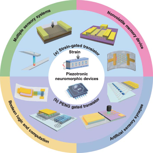
Figure 1. The schematic of diverse structures and applications of piezotronic neuromorphic devices. (a) Strain-gated transistor. (b) PENG gated transistor.
Download figure:
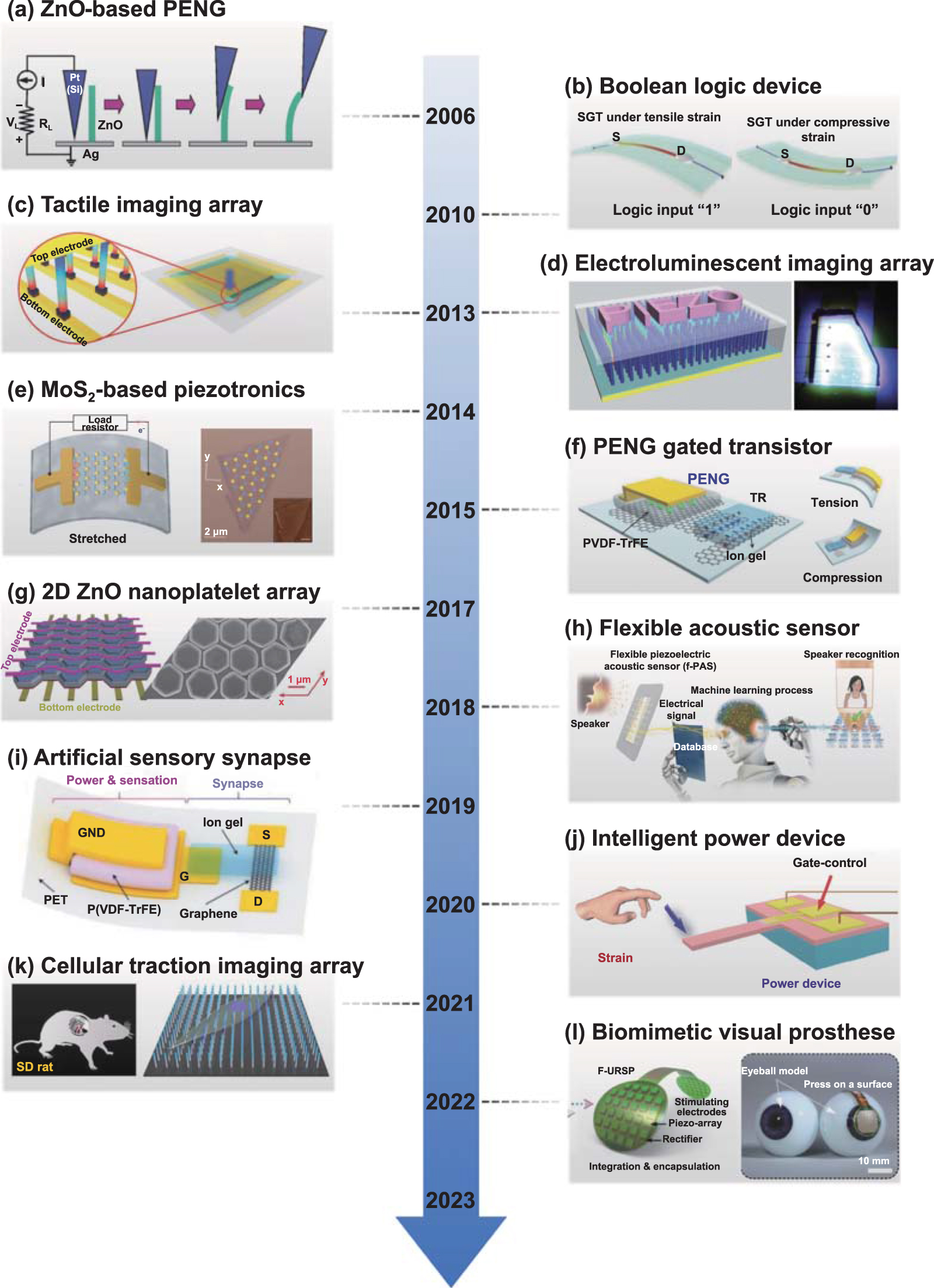
Standard image High-resolution imageFigure 2 shows the timeline of experimental milestones for piezotronic neuromorphic devices [13, 17–27]. Since the proposal of PENGs based on ZnO NW arrays in 2006 [18], the research field of piezotronics has gained continuous and extensive development. This article reviews recent research advances in piezotronic neuromorphic devices and provides a detailed discussion on device structures, operating mechanisms, and fabrication techniques. We also introduce multifunctional applications based on piezotronic neuromorphic devices, including multisensory perception, storage, logic computing, and optical/electrical synapses. Finally, in the context of future development challenges and perspectives, we have further discussed how to modulate novel neuromorphic devices with the piezotronic effect more effectively.
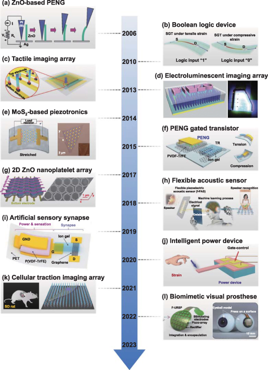
Figure 2. The chronicle timeline showing the experimental milestones for piezotronic devices. (a) ZnO-based PENG. From [18]. Reprinted with permission from AAAS. (b) Boolean logic device. [19] John Wiley & Sons. Copyright © 2010 WILEY‐VCH Verlag GmbH & Co. KGaA, Weinheim. (c) Tactile imaging array. From [20]. Reprinted with permission from AAAS. (d) Electroluminescent imaging array. Reproduced from [21], with permission from Springer Nature. (e) MoS2-based piezotronics. Reproduced from [22], with permission from Springer Nature. (f) PENG gated transistor. [13] John Wiley & Sons. © 2015 WILEY‐VCH Verlag GmbH & Co. KGaA, Weinheim. (g) 2D ZnO nanoplatelet array. [23] John Wiley & Sons. © 2017 WILEY‐VCH Verlag GmbH & Co. KGaA, Weinheim. (h) Flexible acoustic sensor. Reprinted from [24], © 2018 Elsevier Ltd All rights reserved. (i) Artificial sensory synapse. [17] John Wiley & Sons. © 2019 WILEY‐VCH Verlag GmbH & Co. KGaA, Weinheim. (j) Intelligent power device. Reproduced from [25]. CC BY 4.0. (k) Cellular traction imaging array. From [26]. Reprinted with permission from AAAS. (l) Biomimetic visual prosthese. Reproduced from [27]. CC BY 4.0.
Download figure:
Standard image High-resolution image2. The principle of piezotronic effect and piezopotential modulation
Piezoelectric semiconductors have both piezoelectric and semiconducting properties, and most of their crystals are wurtzite with hexagonal structures, such as ZnO, GaN, etc. Taking ZnO crystals as an example, the non-centrosymmetric structure leads to the crystal with a large anisotropy in the c-axis direction, thus endowing it with piezoelectric properties. The centers of the anions and cations are overlapped with each other in the absence of stress action. In contrast, under external stress, the centers of the anions and cations separate from each other and produce an electrical dipole moment, generating a piezoelectric polarization charge along a certain direction inside the crystal [11]. The electrical dipole moments generated by all units in the crystal are superimposed, resulting in a piezopotential along the stress direction on a macroscopic scale [10]. The magnitude of the piezopotential mainly depends on the doping concentration and the applied stress. The strain-induced piezopotential in piezoelectric semiconductors is the basis of PENG and piezotronic transistor, which makes it ready to modulate the electrical properties of piezoelectric transistor with external mechanical stimuli.
When a contact forms between a metal and an n-type piezoelectric semiconductor, due to the different work functions of the metal and the semiconductor, the energy band on the semiconductor surface is bent, resulting in a Schottky barrier at the interface. In the initial state, the degree of energy band bending at the Schottky contact relies on the structural properties of the semiconductor as well as being influenced by the interaction between the metal and semiconductor [28]. The negative piezopotential induced by the tensile strain makes the free electrons in the n-type semiconductor more depleted, resulting in an increased Schottky barrier height (SBH) and leading to the upward bending of the energy band (figure 3(a)). By contrast, the positive piezopotential induced by the compressive strain makes the free electrons in the n-type semiconductor attracted, leading to the downward bending of the energy band (figure 3(b)) [11]. Thus, modulation on the carrier transport behavior in M–S contacts can be realized by strain-induced piezopotential [29–34].
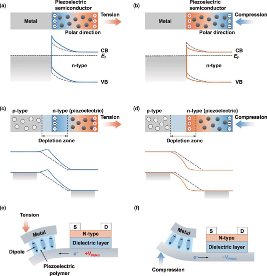
Figure 3. The principle of piezotronic effect and piezopotential modulation. (a) and (b) Piezopotential on metal-semiconductor (n-type) contacts under tensile and compressive strains. (c) and (d) Piezopotential on p-n junction under tensile and compressive strains. Reproduced from [32], with permission from Springer Nature. (e) and (f) the working mechanism of the PENG-gated field effect transistor.
Download figure:
Standard image High-resolution imageWhen a p-type non-piezoelectric semiconductor and an n-type piezoelectric semiconductor form a p–n heterojunction, the holes in the p-type semiconductor and the electrons in the n-type semiconductor near the interface are redistributed and a charge depletion region is formed in the junction region. The strain-induced piezoelectric charge can affect the width of the depletion region and the tilt of the energy band, thus effectively modulating the electron transport in the junction region. Specifically, under the tensile strain, a negative polarization charge is induced on the n-type semiconductor side, and the depletion widths of the n-type and p-type semiconductors increase and decrease, respectively, which causes the depletion region to move toward the n-type side (figure 3(c)) [35]. When the depletion layer on the p-type side narrows to the width of the piezoelectric polarization region, the interaction between the negatively polarized charges and the charge carriers leads to the upward bending of the local band structure [11, 32]. As a contrast, positive polarization charges are induced on the n-type side under compressive strain, and the depletion region moves towards the p-type side, resulting in downward bending of the local band structure (figure 3(d)). This coupling of piezoelectricity and carrier transport properties in piezoelectric semiconductors is known as the piezotronic effect [29, 31, 36]. The piezopotential acts as the gate in piezoelectric semiconductor devices and effectively modulates the electron transport characteristics of the channel. By analyzing the working mechanism of piezopotential on M–S contacts and p–n junctions, piezotronics directly links external strain and electrons transport, creating a new avenue for the design of sophisticated electronic devices capable of sensing external mechanical stimuli toward multifunctional applications.
The PENG-gated three-terminal device is composed of a transistor and a PENG connected to the gate (figures 3(e) and (f)). PENG is usually constructed with a piezoelectric layer sandwiched between two metal electrodes [37], using the electric field generated by the piezoelectric effect to drive the transient flow of electrons in the external circuit. In the initial state, the anions and cations in the piezoelectric material are overlapping. When an external force is applied to the PENG, the volume of the piezoelectric material decreases. The separation of the anion and cation changes the electrical dipole moment and creates a piezopotential between the two electrodes. When the PENG is connected to an external circuit, the piezopotential drives the flow of electrons in the external circuit and reaches an equilibrium condition. When the external force is released, the electrons flow back and eventually result in a new equilibrium condition [38, 39]. In the PENG-gated three-terminal device, the tensile and compressive strains applied on the PENG can induce positive and negative piezopotentials (+VPENG/−VPENG) to couple to the transistor gate, thereby modulating the concentration of charge carriers in the semiconductor channel.
3. Manufacture of active nanomaterials for the neuromorphic piezotronic devices
By coupling piezoelectric and semiconductor properties, piezotronic neuromorphic devices realize precise modulation on electrical performance with pressure or mechanical displacement. Active nanomaterials with 1D or 2D structures in piezotronic neuromorphic devices are essential for proper operation and diverse functionality of the devices. In this section, we will briefly describe two main fabrication methods for active nanomaterials, including the 'bottom-up' and 'top-down' methods.
3.1. Bottom-up fabrication
In nanoscience, the bottom-up method means an extremely small manufacturing process which can grow the desired nanomaterials and structures on a substrate starting from atoms/molecules in a self-assembly fashion. The commonly used bottom-up methods include wet chemical synthesis and chemical/physical vapor depositions.
Generally, the wet chemical methods refer to the synthetic processes to prepare nanomaterials with liquid phase participating in the chemical reaction, including chemical liquid deposition, electrochemical deposition, sol-gel processing, hydrothermal synthesis, etc. The primary principle of wet chemical process is to sophisticatedly select one (or several) required soluble metal salts (or oxides) to prepare the reaction solution according to the composition of target synthetic materials [40–42]. In the reaction solution, the target elements in an ionic or molecular state uniformly precipitate or crystallize to form the required nanomaterials by applying (or crystallizing) suitable precipitants induced by evaporation, sublimation, or hydrolysis.
For the vapor deposition method, high-quality nanomaterials can be deposited on a substrate by using physical or chemical processes, which generally occur in the gas phase. According to the film growth mechanism of vapor deposition technique, it can be classified into chemical vapor deposition (CVD), physical vapor deposition, etc. Commonly, the vapor deposition techniques are accepted by researchers with high reactive temperature environment, expensive instruments, and comprehensive processing because these methods are preferential to fabricate various types of materials that cannot be synthesized by wet chemical synthesis, such as GaN. For instance, high quality NWs, 2D materials, etc, can be readily grown by the CVD method. During the CVD process, target oxide powder is heated in a tubular furnace and evaporated to the upper surface of the substrate by flowing Ar gas and then forming the desired material under specific temperature, pressure, atmosphere, etc. Pulsed laser deposition (PLD) is another common method for growing epitaxial thin films [43]. During the NWs growth process, the ceramic target is bombarded with a high-energy laser, transformed into a plasma, and then deposited on the top surface of the single-crystal substrate. Accordingly, a buffer layer pre-deposited on the substrate is critical to the morphology of the required target nanomaterials. For instance, a textured buffer layer prepared on the single crystal substrate is the key to the fabrication of vertically oriented NWs [44–47].
3.2. Top-down fabrication
Although the bottom-up fabrication is qualified to grow large-scale nanomaterials, it also has some shortcomings, e.g. the nonuniform height, diameter, and composition of the target materials. In contrast to bottom-up method, another fabrication strategy (i.e. top-down method) is well used in the semiconductor industry. The top-down fabrication process refers to the direct preparation of desired nanostructures on the substrate (or bulk material) through a series of thin film deposition, photolithography, and etching techniques. By employing top-down patterning and inductively coupled plasma techniques, highly uniform and well-oriented NWs can be fabricated on a high-quality epitaxial single crystal film [48–51]. The top-down method has also been widely applied to the preparation of devices such as 2D materials-based transistors. For instance, by applying external shear force on the material bulk, the distance between the layers is increased and the van der Waals forces are weakened to realize the exfoliation of 2D crystals.
These two types of synthesis and fabrication methods are highly promising for preparing the active nanomaterials for piezotronic neuromorphic devices. The bottom-up fabrication has shown good compatibility and a wide range of applicability, while the wet chemical synthesis is the least expensive method in terms of both equipment and materials. For vapor deposition, the fast growth rate and large growth area make it suitable for continuous fabrication in laboratory (or industry). Top-down fabrication process is relatively expensive but it is compatible with state-of-the-art semiconductor technology and available for large-scale fabrication, which generally requires large-scale equipment paired with complicated techniques. The elaborate combination of top-down and bottom-up methods is highly required to prepare more sophisticated neuromorphic piezotronic devices in future.
4. Neuromorphic applications of piezotronic devices
The emerging technology of coupling the piezoelectric effect with semiconductor devices shows great potential for neuromorphic applications in the coming intelligent era. Bionic perception/sensing, information storage and computation, and artificial synapses are undoubtedly the focus of research and development direction in the application of piezotronic neuromorphic devices.
4.1. Piezotronic devices for sensing functions
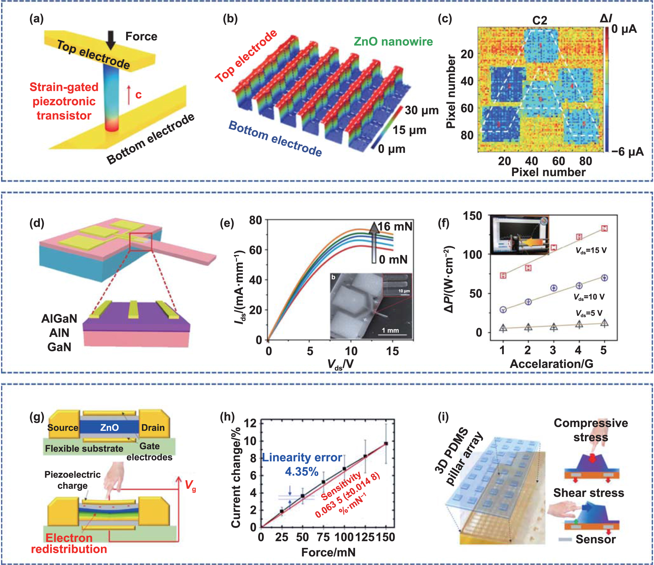
Tactile sensation is an important form of perception in which people acquire information from the surrounding environment. Simulated tactile perception sensors have been developed and widely used in various scenarios. However, the integration and resolution of tactile sensors using piezoresistive or capacitive types are low, which are not suitable for high precision and tiny tactile sensing. By replacing the gate with strain to regulate the channel carriers, Wang's group proposes a two-terminal strain-gated vertical piezotronic transistor (SGVPT), as shown in figure 4(a) [20]. By integrating ZnO NW-based SGVPT into a 92 × 92 addressable pressure sensing array, active and adaptive tactile imaging is achieved. As shown in figure 4(b), the array topology diagram shows the structure and arrangement of the devices. The top and bottom electrodes are gold/indium tin oxide (Au/ITO) constructed in an orthogonal configuration for addressing external pressure stimuli. Gold electrodes and ZnO form Schottky contacts, which act as a piezoelectric gate. A mold in the shape of a letter A is pressed vertically onto the surface of the device with a pressure of 25 kPa. Figure 4(c) shows the corresponding current response contour plot. The device has a high spatial resolution of 234 dpi and a sensitivity of about 2 μS kPa−1, which demonstrates its excellent pressure sensing capability. This interesting structural design based on ZnO NWs provides a new way to construct tactile imaging devices with high spatial resolution. In addition, the spatial resolution of the pressure sensor can be increased to 12 700 dpi based on an ordered array of hexagonal ZnO nanosheets [23]. By integrating a WO3 electrochromic device film and a ZnO-NW matrix pressure sensor, Han et al simultaneously realize the visualization and recording of spatial pressure [52].

Figure 4. Piezotronic devices for tactile sensing. (a) Schematic diagram of a two-terminal SGVPT based on ZnO NWs. (b) Topological diagram of the 92 × 92 piezoelectric transistor array showing the structure and arrangement of the device. (c) Current response contour plot after applying six normal stresses in the shape of the letter A on the transistor array. From [20]. Reprinted with permission from AAAS. (d) Schematic diagram of SPD based on AlGaN/AlN/GaN heterojunction transistors. (e) Output curves of the SPD under different strains. The inset shows the SEM image of the SPD. (f) Output power density of SPD versus acceleration. The inset shows the test process of acceleration-feedback-control. Reproduced from [25].CC BY 4.0. Copyright 2020, Springer Nature. (g) Schematic of haptic sensing using a ZnO TFT. From [53]. Reprinted with permission from AAAS. (h) The output current variation curves of the array under different applied forces. (i) Shear force measurement with TFT arrays.
Download figure:
Standard image High-resolution imageTactile perception based on piezotronic effect can also be applied in smart power devices. Inspired by the human reflex process, Zhang et al propose a high electron mobility transistor with a cantilever structure based on the AlGaN/AlN/GaN heterojunction (figure 4(d)) [25], which can serve as a strain-controlled power device (SPD) to achieve fast modulation of the output power by external mechanical stimulation. As shown in the inset of figure 4(b-ii), the scanning electron microscope (SEM) image shows the cantilever structure of the SPD. Figure 4(e) shows the output characteristics of the SPD under different strains, in which the gate voltage VG is 1 V. The output current density of the cantilever increases under external stress, with a 17.5% increase in output current at 16 mN stress compared to no stress. In addition, VG can also effectively modulate the output current of the cantilever under strain. Based on the SPD, acceleration feedback control (one of the important functions of AI applications) is successfully implemented on a microcontroller (inset of figure 4(b-iii)). The output power density of SPD versus acceleration is shown in figure 4(f). As the acceleration increases (from 1 G to 5 G), the output power increases with self-regulation capability. The proposed SPD has promising applications in AI fields, such as autopilots and intelligent robots.
In tactile perception systems, the perception and detection of pressure in different directions are also necessary. Shadi A. Oh et al prepare a flexible tactile sensing array based on dual-gate piezoelectric ZnO thin film transistors (TFTs) for sensing shear forces and autonomously adjusting closed-loop grasps [53]. For a single ZnO TFT, piezoelectric charges accumulate on the channel surface under the action of vertical forces and lead to a current variation for the output, which enables the perception of tactile sensation (figure 4(g)). Based on the reliable current switching capability of TFTs with dual-gate structure, two 8 × 16 multiplexed tactile sensor arrays are prepared on wafers for pressure mapping. As shown in figure 4(h), the average force response of the 10 different areas in the array is proportional to the magnitude of the applied force. The calculated sensitivity of (0.063 5 ± 0.014 8)%·mN−1 with a linearity error of 4.35% demonstrates the excellent normal stress sensing capability of the TFT. Besides, by using 3D polydimethylsiloxane (PDMS) pillars on multiple force sensors, the lateral shear forces are converted into vertical forces for measurement, enabling the sensing of different force directions and magnitudes (figure 4(i)) [54, 55]. This high spatiotemporal resolution multiplexed tactile sensing array provides a novel approach to constructing normal and shear force sensory devices.
Vision is the sense that provides the most amount of information, so it is important to simulate visual perception for neuromorphic optoelectronics. The piezo-phototronic effect, first proposed in 2010 [11, 56, 57], reflects the coupled response of optoelectronic devices to stress and light, providing a new idea for the integration of multiple senses, such as tactile and visual sensing. Wang et al demonstrate a hybridized photodetector based on p-Si/n-ZnO heterojunction [58], as shown in figure 5(a). The piezoelectric polarization charge induced on the n-ZnO side under strain can effectively modulate the photoelectric effect on the p-Si side, thus improving the optoelectronic performance of the device. The SEM image of the device is shown in the inset of figure 5(a). First, micro-pyramid structures are etched on the p-type silicon wafer to increase the surface area and help to improve the light absorption. Then a ZnO NW layer is covered on the sample surface to form p-Si/n-ZnO heterojunction. Finally, Ag NWs are dispersed on the ZnO array with a sputtered ITO layer as the top electrode. The output current of the p–n junction at different optical power densities and strains is measured and extracted with a fixed bias voltage of 2 V (figure 5(b)). The output current increases significantly with the increase of optical power density and external strain. The performance optimization of silicon-based optoelectronic devices is achieved through a smart integration of strain and illumination, and this general strategy can be applied to various fields.
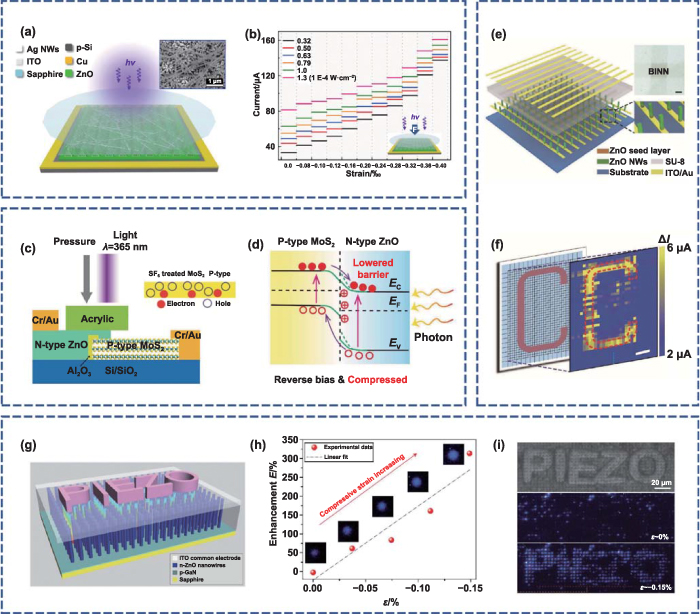
Figure 5. Piezotronic devices for visual sensing. (a) Schematic diagram of the structure of the p-Si/n-ZnO heterojunction photodetector. The inset shows the SEM image of the device. (b) The output current statistic of the photodetector under different light and strain conditions. The inset shows the schematic diagram of the experimental setup for light and strain coupling. Reprinted with permission from [58]. Copyright (2014) American Chemical Society. (c) Schematic diagram of the piezo-phototronic effect in a MoS2/ZnO heterojunction-based photodiode. (d) Energy band diagram of p-MoS2/n-ZnO under reverse bias and compression conditions. [59] John Wiley & Sons.© 2016 WILEY‐VCH Verlag GmbH & Co. KGaA, Weinheim. (e) Schematic diagram of the ZnO NW-based UV photodetector array. (f) Output current mapping for distribution imaging of UV illumination under strain of 40.38 MPa. [60] John Wiley & Sons.© 2015 WILEY‐VCH Verlag GmbH & Co. KGaA, Weinheim. (g) The NW-LED-based pressure sensor array. (h) The enhancement E as a function of the applied compressive strain, and the corresponding luminescent device diagram. (i) The optical image of the stamp and the luminescent image of the device with applied strains of 0 and −0.15%. Reproduced from [21], with permission from Springer Nature.
Download figure:
Standard image High-resolution imageThe piezo-phototronic effect can also influence the performance of p–n junction photodetectors. Xue et al demonstrate a p–n photodiode based on MoS2/ZnO heterojunction, and the structure schematic is shown in figure 5(c) [59]. The p-type MoS2 films are obtained by exfoliating from bulk crystals and treated with SF-6 plasma, and the n-type ZnO films are deposited on the wafer surface by PLD. The transparent acrylic above the heterojunction can detect the amount of applied pressure and has little effect on the incident UV light. The piezo-phototronic effect can enhance the photoresponse of p-type MoS2 and n-type ZnO photodiodes. Figure 5(d) shows the energy band diagram of the photocurrent enhanced by the piezo-phototronic effect. Under a reverse bias and light illumination, the Fermi levels of MoS2 and ZnO will generate an energy difference, which is beneficial to the separation of photogenerated carriers. When external pressure is applied to the device, the positive and negative piezoelectric charges are separated along the c-axis, causing the energy band on the ZnO side to bend downward. This enables the regulation of the diode photocurrent by external pressure.
The vertical array structure contributes to higher computational speed and lowers the chip size and power consumption [61]. Han et al propose a UV photodetector array based on ZnO NWs (32 × 40 pixels, figure 5(e)) [60], in which the top and bottom ITO/Au electrodes are vertically aligned, and the Au and ZnO NWs form Schottky junctions. Strain-induced piezoelectric polarization charges can enhance the optoelectronic properties of ZnO NWs arrays. The imaging of the output current of the ZnO NWs array upon UV illumination is measured under the circumstances of strain-free and 40.38 MPa pressure, respectively (the UV illumination intensity is 1.38 mW cm−2 and the applied bias voltage is 1 V). Figure 5(f) shows the current difference between the two imaging results, which indicates that the output current of the photodetector array increases significantly under applied pressure. With the piezo-phototronic effect, the UV photodetector array has achieved a 700% increase in photoresponsivity and a 600% increase in sensitivity, which provides an essential method for designing high-performance optoelectronic devices.
The piezo-phototronic effect is also used to enhance the light-emitting properties of optoelectronic devices. Pan et al construct a NW light-emitting diode (NW-LED) array for electroluminescent imaging with a spatial resolution of 2.7 μm (figure 5(g)) [21]. By growing n-type ZnO NWs on p-type GaN thin film substrates, an array of p–n junction light-emitting devices is formed. Under forward bias, the luminescence performance of each pixel is modulated by the strain magnitude. Figure 5(h) shows the enhancement E of the NW-LED as a function of the applied compressive strain, together with the corresponding luminescent status. The enhancement E reflects the change in the luminescence intensity of the device, which is proportional to the magnitude of the compression strain. When a 'PIEZO'-shaped stamp is pressed on the NW-LED array, figure 5(i) shows the corresponding optical image of the stamp and the luminescent image of the device under applied strain of 0 and −0.15%. This NW-LED array converts external mechanical signals into electroluminescent signals to visually reflect the distribution of applied pressure, enabling efficient data transmission and processing.
In addition to tactile and visual perception, other sensing modals can also be modulated by piezotronic effects. As one of the important sensory channels, hearing is the most direct way of receiving information during human/robot communication. As shown in figure 6(a-i), Han et al demonstrate a flexible piezoacoustic sensor (f-PAS) that implements speaker recognition based on a machine learning process [24]. Flexible PZT films with piezoelectric properties are transferred to a polymer substrate, and the concaved trapezoidal structure mimics the basement membrane in the human cochlear (figure 6(a-ii)). Seven channels of the interdigitated electrodes are defined by photolithography and etching processes. The vibrations induced by the human voice trigger the multi-channel piezoelectric current signal, which is a self-driven process. Using machine learning to extract the frequency features of speech signals and train them to achieve speaker recognition, figure 6(a-iii) shows the speaker recognition error rate statistics of f-PAS and commercial microphones for 30 mixed samples. The recognition error rate of two-averaging is only 2.5%, which demonstrates the excellent recognition capability and potential application advantages of f-PAS.
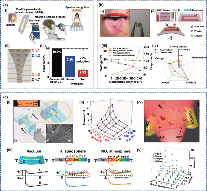
Figure 6. Piezotronic devices for other modal sensations. (a) The f-PAS for speaker recognition. Reprinted from [24], © 2018 Elsevier Ltd. All rights reserved. Copyright 2018, Elsevier. (b) The self-powered gustation electronic skin based on enzyme-modified ZnO nanowire arrays. Reproduced from [62]. © IOP Publishing Ltd All rights reserved. (c) Gas sensors for simulating olfactory perception. (i)–(iii) The piezotronic-enhanced gas sensors based on ZnO NW for the detection of H2 and NO2. Reprinted from [63], Copyright © 2015 Elsevier Ltd All rights reserved. (iv)–(v) The flexible NO2 gas sensors based on single-layer MoS2. Reprinted from [64], © 2018 Science China Press. Published by Elsevier B.V. and Science China Press. All rights reserved.
Download figure:
Standard image High-resolution imagePiezotronic neuromorphic devices have also been used to simulate taste perception. Zhao et al propose a self-powered electronic skin to achieve taste perception function by enzyme-modified ZnO NW arrays [62]. As shown in figure 6(b-ii), the device is composed of ZnO NWs and interdigitated electrodes, which can output a continuous piezoelectric signal through the piezoelectric-enzymatic reaction coupling effect. By modifying ZnO NWs with ascorbate acid oxidase (AAO), figure 6(b-iii) shows the piezoelectric output voltages and responses of ZnO and AAO@ZnO NWs after adding 5 ml of ascorbic acid (AA) solution to 20 ml of pure water. Compared with the unmodified ZnO NWs, the response of AAO@ZnO NWs to the AA solution is significantly enhanced, which demonstrates the favorable recognition of AA by the devices. In addition, the self-powered electronic skin is used to detect the AA concentration of different fruits (figure 6(b-iv)). Enzyme-modified ZnO NW arrays provide a new approach to achieving gustatory perception.
Gas sensors are capable of converting the composition and concentration information of the measured gas into electrical signals [65], which can be considered as simulated olfactory perception. Zhou et al propose a piezotronic effect enhanced gas sensor based on ZnO NW, which can be used to detect hydrogen (H2) and nitrogen dioxide (NO2) gases (figure 6(c-i)) [63]. By applying strain to the ZnO NW through the displacement of a linear motor, they have successfully modulated the sensor sensitivity and realized the gas detection at room temperature. Figure 6(c-ii) shows the current variation of the device under H2 atmosphere and compressive strain conditions. An increase in either H2 concentration or strain results in a higher output current, which reflects the high sensitivity and resolution of the gas sensor. The energy band diagram reflects the operating principle of the ZnO NW gas sensor (figure 6(c-iii)). Under compressive strain, the energy band of ZnO bends downward. When H2 gas is passed into the cavity, the H2 molecules dissociate by reacting with O2−, and electrons are injected into the conduction band and accumulate on the ZnO surface, which increases the response current. By contrast, when NO2 gas is passed into the cavity, the NO2 molecules associate with the oxygen vacancies. Electrons are discharged from the conduction band to induce a depletion layer on the surface, which reduces the output current of the device. Thus, the piezotronic effect can improve the performance of gas sensors by changing the energy band structure of the M–S interface.
In addition, piezo-phototronic effects in 2D semiconductors are also used in gas sensing applications. Guo et al propose a flexible NO2 gas sensor based on MoS2 FET (figure 6(c-iv)) [64], and the current variation of the device reflects the ability of gas sensing. The device is obtained by transferring single-layer MoS2 grown by CVD to a flexible PET substrate with defined source and drain electrodes on both sides. As shown in figure 6(c–v), when the NO2 concentration is 400 ppb, the sensitivity of the device is improved to 671% under the tensile strain of 0.67% and the 625 nm optical illumination of 4 mW cm−2 (compared with no strain and light conditions). In addition, the response/recovery time of the sensor for NO2 gas is reduced considerably. The combination of excellent physical properties of 2D materials and piezoelectric effects facilitates the construction of highly sensitive gas sensors.
4.2. Piezotronic devices for information storage and computation
In addition to simulating biological perception, piezotronic neuromorphic devices are required to have the function of data memory/storage after receiving and converting the external stimulus signals. For instance, the modulation of the metal-electrolyte interface by the piezopotential can impact the memory switching characteristics of a memristor [2, 66–68]. Wu and Wang construct the first resistive switching device by using ZnO NW [69], which effectively modulates the memory properties of resistive memory cells by strain (figure 7(a)). When ZnO NW is subjected to external stress, the hysteretic I–V characteristics of the resistive memory cell change accordingly. As shown in figure 7(b), when the device is under tensile strain ( = 1.17%), the hysteretic switching curve shifts in the negative voltage direction; when the device is under compressive strain ( = −0.76%), the I–V characteristic curve shifts in the positive voltage direction. Vth,S and Vth,D represent the threshold switching voltages in the I–V characteristic curves, which will increase or decrease according to the applied strain (figure 7(c)). It should be noted that the window width of the threshold voltage remains almost constant under different strain states. The demonstrated ZnO NW-based nonvolatile resistive switching memories have a large range of applications.

Figure 7. Piezotronic devices for information storage. (a) The resistive switching device based on piezotronic ZnO NW. (b) I–V characteristic curves of the device under tensile, zero, and compressive strains. (c) Threshold switching voltage versus applied strain. Reprinted with permission from [69]. Copyright (2011) American Chemical Society. (d) The piezotronic memristor based on bamboo-like GaN micron wires. (e) I–V characteristic curves of the piezotronic memristor under different compression strains. (f) The SET voltages at different strains extracted from (e). [70] John Wiley & Sons.© 2016 WILEY‐VCH Verlag GmbH & Co. KGaA, Weinheim. (g) Schematic of sensory memory system in skin and GaN piezotronic memory under compressive strain. (h) The typical I–V characteristics of the piezotronic memory before and after applying strain. (i) The endurance characteristics of piezotronic memory for 100 cycles. Reprinted from [71], © 2020 Elsevier Ltd All rights reserved.
Download figure:
Standard image High-resolution imageIn addition, Liu et al construct piezotronic memristors with multilevel switching characteristics by synthesizing bamboo-like GaN micro-wires via CVD method [70]. Figure 7(d) shows the schematic of the memristor and the SEM image of the GaN micro-wires. Typical GaN micro-wires have distinct bamboo-shaped knots, which are formed by nucleation and radial growth of GaN in the form of seed crystals during the growth process. The memory switching characteristics of piezotronic memory resistors are mainly attributed to nitrogen-deficient defects in the GaN knot region [72, 73]. By applying compressive strain to the device using a 3D mechanical stage, they explore the influence of the piezoelectric effect on the performance of GaN memristors. Figure 7(e) shows the I–V characteristic curves of the piezotronic memristor under different compressive strains, which exhibit a larger set voltage (the process of switching the device from high resistance state (HRS) to low resistance state (LRS)) at larger compressive strains. Figure 7(f) shows the set voltages at different strains extracted from figure 7(e). As the applied compression strain increases from 0 to −0.76%, the set voltage increases from 1.42 to 2.15 V. Piezotronic memristors can readily optimize the storage performance by modulating the operating voltage through piezotronic effects.
Sensory memory can hold transient stimuli signals for a short period of time, which is essential in individuals' real-time interaction with the environment [74]. As shown in figure 7(g), after receiving an external stimulus, skin receptors are able to store and retain sensory information for certain time, mainly determined by the action of sensory receptors and memory units. Inspired by the skin memory process, Hua et al propose a piezotronic sensory memory based on a single gallium nitride (GaN) microwire [71], which realizes the implementation of sensory and memory functions on a single device. Figure 7(h) shows the typical I–V characteristics of the piezotronic memory before and after applying strains. When applying −1.57% compressive strain to the device, the current of the device in the I–V curve decreases significantly, which indicates that the resistance of the device transitions from LRS to HRS. When the compressive strain is released, the I–V curve remains essentially constant and the resistance maintains at HRS. This demonstrates the good resistive memory capability of the piezotronic memory. In addition, the device's resistance can be reversibly returned to the LRS by applying a positive erase voltage. As shown in figure 7(i), the endurance characteristic of the piezotronic memory for 100 cycles is measured under writing process with a strain of −1.57% and erasing processing with the electrical voltage at 3 V. Piezotronic sensory memory enables tactile retention in a single micro/NW, contributing to the development of interactive neuromorphic devices and memories.
The transfer characteristics of the piezotronic strain-gated transistor (SGT) can be directly modulated by the applied external stress. The integration of multiple SGTs is expected to enable multiple logic operation functions for stress control. As early as 2010, Wu et al first implement piezotronic logic operations with ZnO NWs [19]. With continuous research and development on piezotronic logic devices, piezotronics is being broadened to various piezoelectric materials toward more sophisticated applications. Yu et al propose a piezotronic SGT based on GaN nanoribbons and demonstrate the universal logic operation [75]. As shown in figure 8(a), they prepare GaN nanoribbons in uniform size by strain-controlled cracking of GaN films, and then fix the two ends of GaN nanoribbons with silver paste as the source and drain electrodes of the device. The inset of figure 8(a) shows the optical image of the GaN nanoribbon piezotronic SGT. Based on the piezotronic effect of GaN, the output current of the piezotronic SGT exhibits 'off' and 'on' states under tensile and compressive strains, respectively (under a fixed bias). The piezotronic inverter is made by encapsulating two GaN nanoribbon SGTs on the same substrate. Figure 8(b) shows the variation of the output voltage of the piezotronic inverter for different strain inputs, where logical '0' and '1' are obtained for positive and negative strains, respectively. In addition, other logic operations, including AND, OR, NAND, NOR, and XOR gates, can also be implemented based on the SGT device with GaN nanoribbon. This concept of strain-gated piezotronic logic has great potential for application in intelligent electronic devices.
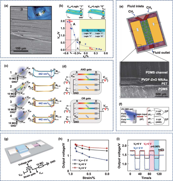
Figure 8. Piezotronic devices for logic computation. (a) GaN nanoribbon based strain-gated piezotronic transistor. (b) The relationship between input strain and output voltage exhibits the function of a logic invertor. Reprinted with permission from [75]. Copyright (2013) American Chemical Society. (c) Schematics and energy band diagrams of the CdS NW-based light/strain-gated transistor. (d) Light/strain-controlled piezo-phototronic AND and OR logic gates. [76] John Wiley & Sons.© 2014 WILEY‐VCH Verlag GmbH & Co. KGaA, Weinheim. (e) The schematic of Y-OF and the SEM image of layer-by-layer structure. (f) The simplified schematic of Y-OF implemented OR logic gate and AND logic gate. Reproduced from [77]. CC BY 4.0. (g) Schematic diagram of the piezotronic logic inverter based on ion-gel-gated ZnO NW. (h) Output voltage versus strain at different gate voltages. (i) The V-t characteristics of the piezotronic logic inverter under periodic strain. [78] John Wiley & Sons.© 2019 WILEY‐VCH Verlag GmbH & Co. KGaA, Weinheim.
Download figure:
Standard image High-resolution imageThe piezo-phototronic effect can provide a more flexible and convenient modulation strategy for logic computing devices. Due to the visible light response and inherent piezoelectric properties of cadmium sulfide (CdS), Yu et al prepare an light-strain-gated transistor (LSGTs) based on CdS NWs [76]. Controlling the carrier transport process by piezo-phototronic effect, figure 8(c) shows the schematic diagram of LSGT and corresponding energy band under optical and mechanical stimulation. The SBH at the interface between CdS and the two terminal electrodes is reduced under illumination, resulting in a significant enhancement of the photocurrent (figure 8(c–i)). Under compressive strain, the positive and negative piezoelectric polarization charges appear near the interface at both terminals, making the potential barrier height of the source contact decreases while the potential barrier height of the drain contact increases (figure 8(c-ii)). When the light and strain are applied simultaneously, the strain magnitude affects the transport behavior of the photogenerated carriers. A small compressive strain (e.g. −0.24%) can help to alleviate the recombination of light-induced electron-hole pairs, resulting in an increased photoconductivity of the CdS NW device (figure 8(c-iii)). At large compressive strains, the valence band edge of the CdS NW is above the Fermi level of the contact electrode and the separation of light-induced electron-hole pairs is suppressed, which thereby leads to a significant reduction in photoconductivity (figure 8(c-iv)). Due to the significant changes in the conductance of LSGTs under applied light and strain, the light/strain-controlled piezo-phototronic logic gates such as 'AND' and 'OR' can be implemented as shown in figure 8(d). The logic '0' of the light input Lin is defined to apply light to #2 and #4 LSGTs, while the logic '0' of the mechanical input in is defined to apply strain to #1 and #2 LSGTs. The optical and mechanical logic '1' is defined as the application of light or strain to the remaining two LSGTs, and the logic output is the amplitude of the output voltage. Other universal logic units have been successfully demonstrated by designing different electrical circuits. Piezo-phototronic circuits provide a new idea for the construction of logic computing devices.
Optofluidic nano/microsystems combine microfluidic and optical technologies to achieve great progress in the large-scale integration of optoelectronics. Purusothaman et al propose a piezopotential modulated optofluidic logic device [77]. Figure 8(e) shows the schematic of Y-channel optofluidic device (Y-OF) and the SEM image of layer-by-layer structure. The sensing layer is made by in-situ growth of zinc oxide nanorods (ZnO NR) on a polyvinylidene fluoride (PVDF) substrate, which can detect three sources of optical, fluidic, and strain stimuli. The fluid flows from two inlet channels (CH1/CH2) of the Y-shaped PDMS groove, converges on the PVDF/ZnO NR surface, and then flows out. Figure 8(f) shows a simplified schematic of the Y-OF implemented OR logic gate and AND logic gate. Two kinds of solvents (e.g. ethanol and decanol), can be identified as logical '0' and logical '1' according to the high and low response of the photocurrent. Only when the ethanol flows as a fluid source in both channels, the photocurrent of the Y-OF is low, corresponding to the OR gate condition '0:0 = 0'. When other combinations of fluid sources flow through the channels, the photocurrent of Y-OF will be higher, corresponding to the OR gate conditions '1:0 = 1', '0:1 = 1', and '1:1 = 1'. Therefore, the Y-OF can achieve OR gate under unstrained conditions. In contrast, the photocurrent response of Y-OF under compressive strain (−1%) will be different. For instance, the photocurrent will be high only when decanol flows as a fluid source in both channels, while it will be lower than the threshold in other combinations of fluid sources. Accordingly, the Y-OF can achieve AND gate under compressive strain. The system integration of optofluidics and piezoelectricity enables convenient switching of multiple logic functions, which contributes to the development of interactive optoelectronics.
Yang et al propose a low-power method for coupling ion-gel gating with piezoelectric effects by exploiting ZnO NW and ion-gel dielectrics [78]. As shown in figure 8(g), a tunable piezotronic logic inverter is constructed by connecting a 10 MΩ resistor in series to an ion-gel-gated ZnO NW device. Figure 8(h) shows the strain versus output voltage (VOUT) at different gate voltages (VG = 0, 2, and −2 V). The variation of VOUT with strain is larger at negative gate voltage than at positive or zero gate voltage. By periodically applying and removing 0.96% tensile strain to the ZnO NW at different gate voltages, the real-time VOUT of the logic device is shown in figure 8(i). The states with no strain and with 0.96% tensile strain applied are considered as '0' and '1' of the logic input, respectively. VOUT decreases significantly after applying a tensile strain, enabling a logic transition from '1' state to '0' state, which corresponds to the NOT gate. The gate voltage can affect the variation of VOUT in the NOT gate. VOUT increases from 0.69 V to 1.48 V at a VG of −2 V, with an increase of 97.5%. The modulation of the logic inverter is implemented by the combination of ion-gel gate control and piezotronic effect, which provides a novel approach to realizing low-power and sophisticated piezotronic devices.
4.3. PENG-gated transistor
Except the piezopotential interface modulation for conventional piezotronic devices, a series of general-conceptual piezotronic devices can be regarded as various electronic devices gated/driven/modulated by PENG. In this way, more abundant piezoelectric polymers with good flexibility and low-temperature processability can be utilized to fabricate multifunctional sensory devices. The coupling behavior between piezoelectric polarization and semiconductor transport properties can also be used to emulate an artificial sensory neuron (or afferent nerve) to implement parallel sensation and computation on the external mechanical stimuli. The neuromorphic devices based on PENG-gated transistors have attracted much attention in recent years due to the advantages of self-powering and directly sensing external stimuli. Sun et al propose a PENG-gated graphene transistor and construct an active strain sensor array [13]. The device consists of a polyvinylidene fluoride-trifluoroethylene [P(VDF-TrFE)]-based PENG and an ion-gel-gated graphene transistor, in which the graphene electrode on the bottom of the PENG is connected to the ion-gel layer of the transistor (figure 9(a)). The strain-induced piezopotential in the PENG is coupled to the gate of the transistor, which effectively modulates the Fermi level of the graphene channel and changes the carrier concentration. Figure 9(c) shows the output characteristics of the graphene transistor when the PENG is under different strain conditions. As the tensile strain increases, the drain current of the transistor increases. Figure 9(d) shows the dynamic current response of the PENG-gated graphene transistor under 0.06% tensile strain and −0.06% compressive strain, which demonstrates a significant and fast feedback to the piezopotential. The strain sensor exhibits excellent sensitivity at lower strains (figure 9(e)). In addition, an active strain sensor array is constructed based on PENG-gated graphene transistors. The output currents in different regions of the array under the diagonal direction of strain are shown in figure 9(b), and the magnitude of the output currents indicates the distribution of strain.
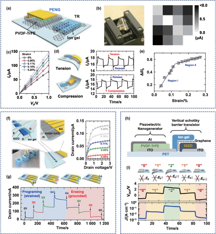
Figure 9. PENG-gated transistor. (a) Schematic of the PENG-gated graphene FET. (b) Schematic of the active-matrix strain sensor array and corresponding output current distribution. (c) Output characteristics of the PENG-gated graphene FET under different strains. (d) The dynamic current response of the PENG-gated graphene FET under tensile and compressive strains. (e) Sensitivity characteristics of the strain sensor [13]. John Wiley & Sons.© 2015 WILEY‐VCH Verlag GmbH & Co. KGaA, Weinheim. (f) The piezopotential-controlled nonvolatile memory array and output characteristics under strain. (g) The multilevel storing/erasing steps of the piezopotential-controlled memory. Reprinted with permission from [14]. Copyright (2016) American Chemical Society. (h) Cross-sectional schematic of the piezotronic graphene barristor. (i) Real-time current density of piezotronic graphene barristor under different strains from two integrated PENGs. Reprinted from [79], © 2018 Elsevier Ltd All rights reserved.
Download figure:
Standard image High-resolution imagePENG-gated FETs can also be used in mechanical information storage. A piezopotential-controlled nonvolatile memory array and the output characteristics under strain are shown in figure 9(f) [14]. The channel material of the FET is indium gallium zinc oxide (IGZO), and the piezoelectric layer of the PENG is P(VDF-TrFE) material. The piezopotential generated by the PENG under strain applies programming and erasing operations to the memory, resulting in lower power consumption of the device. The output characteristic curves under different strains demonstrate the favorable strain sensitivity of the device. Figure 9(g) shows the multilevel storing/erasing steps of the piezopotential-controlled memory by coupling four PENGs to the same ion-gel gate dielectric of the FET. The programming operation can be applied sequentially to each PENG by applying strain and disconnecting the ground terminal of the electrode. And the erasing operation is performed by connecting the electrodes of each PENG to the ground sequentially. The retention of drain current at different levels demonstrates the excellent multilevel data storage performance of the device.
By using the similar strategy, the piezopotential of the PENG can also be used to modulate the Schottky barrier in a graphene barristor. The device includes the PENG with a P(VDF-TrFE) piezoelectric layer and a vertical Schottky barrier transistor with a graphene/IGZO/ITO structure (figure 9(h)) [79]. Based on the capacitive coupling of P(VDF-TrFE) and graphene by ion-gel dielectrics (resulting in electric double layers (EDLs) at the ion-gel interfaces), the piezopotential induced by the strain of PENG can effectively modulate the work function of graphene. The multilevel modulation of the Schottky barrier and the current density of the channel are achieved by coupling two PENGs to the graphene electrode of the same device (figure 9(i)). When a PENG generates a positive piezopotential under tensile strain (0.08%), the Fermi level of graphene moves upward and the current density of the device increases. Meanwhile, the same tensile strain is applied to another PENG, and the Fermi level of graphene moves further upward, and the current density of the device exhibits a stepwise rise. When the strains of the two PENGs are released sequentially, the Fermi level of graphene moves downward to achieve reversible modulation on the current density.
4.4. Piezotronic devices for artificial synapses
The realization of high-performance artificial synaptic electronics is crucial for neuromorphic computing [80]. In the human sensory system, tactile receptors receive external mechanical stimuli and cause the variations of action potential, which are subsequently transmitted to the central nervous system via neurons and synapses (figure 10(a)) [17]. Inspired by the biological sensory system, Chen et al propose a piezotronic graphene artificial sensory synapse as shown in figure 10(b). The system consists of two parts, in which the PENG is used for energy supply and pressure sensing, while the ion-gel-gated transistor is used to simulate synaptic behavior. The piezopotential triggered by external mechanical stimuli causes the formation of EDLs in the ionic gel, which modulates the carrier concentration in the channel and induces changes in the postsynaptic current (PSC). The synaptic characteristics exhibited by ion-gel-gated transistors can be affected by different strain conditions. Figure 10(c) shows the excitatory postsynaptic currents (EPSCs) of the artificial sensory synapse at different magnitudes of stretching strain (0.05%–0.8%). As the applied tensile strain gradually increases, the peak value of the EPSC increases. Temporal and spatial information such as externally applied strain amplitude and duration can be deduced and identified by the EPSC signal. This flexible and self-powered artificial sensory synapse enables direct perception of external stimuli and efficient modulation by piezoelectric effects.

Figure 10. Piezotronic devices for electrical artificial synapses. (a) Schematic of the human sensory nerve system. (b) Device structure of piezotronic graphene artificial sensory synapse. (c) EPSC under different tensile strains. [17] John Wiley & Sons.© 2019 WILEY‐VCH Verlag GmbH & Co. KGaA, Weinheim. (d) Self-powered artificial nerve synapse based on NKN films. (e) Applying a priming spike to achieve metaplasticity of STDP. Reproduced from [16]. CC BY 4.0. (f) Schematic diagram of the ASMS. The piezoelectric device acts as a tactile sensor connected to the ASAN based on NbOx Mott memristors. (g) Input voltage versus response frequency of the ASAN. (h) Frequency response of ASMS at different pressure intensities. Reproduced from [81]. CC BY 4.0.
Download figure:
Standard image High-resolution imageIn addition to replacing the gate voltage in the transistor, the piezopotential generated by the PENG can directly supply energy to the two-terminal device to realize self-driven neuromorphic devices. Kim et al propose an artificial synapse for self-powered biomedical devices [16]. The amorphous (Na0.5K0.5)NbO3 (NKN) thin films possess favorable piezoelectric properties and biocompatibility. The device consists of a Pt/NKN/TiN structured memristor and an NKN-based PENG, which are connected via a bridge rectifier circuit (figure 10(d)). Under the pressure of a finger, the NKN PENG generates an output voltage of more than −2 V to drive the NKN memristor. The NKN memristor exhibits typical synaptic behavior, including short-term plasticity and long-term plasticity (LTP), which is attributed to the movement of oxygen vacancy and changes in the shape of oxygen vacancy filaments in the NKN. Metaplasticity refers to the application of priming stimuli to modify synaptic plasticity before the application of a primary spike to induce synaptic behavior. The priming spike modulation on the metaplasticity is reflected in the spike time-dependent plasticity as shown in figure 10(e). The combination of NKN-based PENG and memristor provides a feasible strategy for applications in biomedical and human-machine interaction fields.
Zhang et al propose an artificial spiking afferent nerve (ASAN) based on NbOx Mott memristors, and build an artificial spiking mechanoreceptor system (ASMS) with a piezoelectric device as the tactile sensor (figure 10(f)) [81]. Pressing and lifting of the finger can generate positive and negative voltage signals in the piezoelectric device. And the produced sinusoidal voltage signal is fed into the ASAN and converted to a peak signal. The input voltage of the ASAN as a function of response frequency is shown in figure 10(g), exhibiting excitability under low input voltages and protective inhibition under high input voltages. Figure 10(h) shows the frequency response of the ASMS under different pressure intensities. The high peak voltage causes the ASAN to stop peaking (protective behavior) under applied high pressures. By combining piezoelectric devices with artificial afferent nerves, external sensory signals are successfully converted into dynamic spike frequencies.
Due to the inherent piezotronic and piezo-phototronic effects of the piezoelectric semiconductor materials in artificial synaptic devices, the synaptic plasticity can be easily modulated by external mechanical stimuli and illumination. Hua et al propose a piezotronic synapse based on a single GaN microwire for strain sensing and synaptic functions [82]. The structure of the artificial synapse and the principle of piezotronic modulation are shown in figure 11(a). The hexagonal GaN NW can generate piezopotential under strain to achieve tactile sensing. More importantly, the piezotronic effect can effectively modulate the synaptic behavior of GaN microwire, which is mainly because the nitrogen vacancies at the junction region are redistributed on the positive charge side under the effect of stress-induced piezopotential. Figure 11(b) shows the current response of the artificial synaptic device to a voltage pulse (2.5 V, 1 ms). When the pulse voltage is reduced to 0.1 V, the output current gradually decays over a period of time, which is mainly attributed to the process of re-releasing the trapped electrons after the withdrawal of the electric field. The decay process of the current can be fitted accurately with an exponential function (the inset of figure 11(b)). The synaptic weights versus the voltage pulse number (2.7 V, 1 ms, Δt = 3 ms) under different strains are shown in figure 11(c). When the strain is increased from 0 to −0.36%, the synaptic weight of the piezotronic synaptic device increases significantly by 330%. In addition, artificial synaptic devices based on ZnO NW can also be modulated by both piezotronic and piezo-phototronic effects. By coupling the piezotronic effect with the optoelectronic properties, Hu et al propose a flexible photonic synapse constructed by a single ZnO micro/NW (figure 11(d)) [83]. The conductance changes of the synaptic device under the impact of light pulses match the behaviors of biological synapse, and the strain-induced piezopotential can effectively modulate the synaptic plasticity. The I–V characteristic curves of the device are modulated by the applied strain and 365 nm UV light (figure 11(e)), exhibiting a significant increase in photocurrent at −0.18% compressive strain and illumination. The contact properties between ZnO and silver paste electrodes lead to a nonlinear fluctuation of the curve [32, 57, 63]. As shown in figure 11(f), the conductance exhibits a gradual increase of enhanced synaptic plasticity under the action of 10 consecutive light pulses (0.227 mW cm−2, 1 s, Δt = 1 s), and the applied compressive strain can promote the increase of conductance.

Figure 11. Piezotronic devices for optical artificial synapses. (a) Schematic diagram of the GaN microwire-based piezotronic artificial synapse and the piezotronic modulation principle. (b) Current response of the device after applying a voltage pulse (2.5 V, 1 ms). (c) Synaptic weights versus the number of voltage pulses (2.7 V, 1 ms, Δt = 3 ms) under different strains. Reprinted with permission from [82]. Copyright (2020) American Chemical Society. (d) Schematic diagram of the photonic synapse based on ZnO micro/nanowire. (e) I–V characteristic curves of photonic synapses under the applied light of 0.468 mW cm−2 intensity and different magnitudes of compressive strain. (f) Conductance changes of synaptic devices induced by 10 consecutive light pulses under different compressive strains. Reprinted from [83], © 2021 Published by Elsevier Ltd. (g) NiO/ZnO-based piezoelectric artificial synapses and the energy band diagram of the p–n junction under strain. (h) Current response of continuously applied 50 positive voltage pulses and 50 negative voltage pulses under different strains. (i) PPF index versus time interval of the pulse under different strains. Reprinted from [84], © 2020 Elsevier Ltd All rights reserved.
Download figure:
Standard image High-resolution imageKumar et al propose an artificial sensory synapse based on NiO/ZnO p–n junction for neuromorphic tactile perception [84]. The structure and energy bands of the peroxide-based artificial synapse under high strain are shown in figure 11(g). The device has a vertically aligned structure and bends in response to external mechanical stimuli. As the applied strain increases, more charges are trapped at the interface of the NiO/ZnO p–n junction, thus realizing the modulation of synaptic behavior with strain. Figure 11(h) shows the modulation of multipulse synaptic plasticity by the applied strain. When 50 consecutive positive voltage pulses (+2 V, 2 ms, Δt = 2 ms) and 50 negative voltage pulses (−2 V, 2 ms, Δt = 2 ms) are applied, the device exhibits typical LTP and long-term depression behaviors. In addition, the PSC increases significantly as the strain increases from 0 to 0.6%. Similarly, the paired-pulse facilitation (PPF), a major important characteristic in biological synapses, can be well modulated by strain. The PPF index increases as the pulse interval time decreases and it is enhanced by the applied strain (figure 11(i)). As previously mentioned, NiO/ZnO-based artificial synapses can be efficiently modulated by external mechanical stimuli, which contributes to the development of low-complexity and low-power neuromorphic tactile perception systems.
5. Summary and perspectives
The technology for effective modulation of neuromorphic devices using piezopotential based on piezotronics devices and strain/PENG-gated transistors has made significant progress in recent years (i.e. piezotronic neuromorphic devices). The basic principle of the device is to use the piezoelectricity of the semiconductor material itself or connect an external PENG to the neuromorphic transistors, thus replacing the gate voltage with the piezopotential (formed by the piezoelectric polarized charges) to control the electrons transport. The piezotronic neuromorphic device innovatively uses a piezopotential gating method to directly correlate the external spatiotemporal mechanical input signal with the electrical output signal. In addition, the application of piezotronic neuromorphic devices has also been significantly broadened by exploiting the piezoelectric material property or structure design. This article systematically reviews the basic principles, manufacturing techniques, and modulation strategies of piezotronic neuromorphic devices and summarizes their applications in bionic sensing, information storage, logic computing, and artificial electrical/optical synapses.
Although these recent developments in various aspects have brought piezotronic neuromorphic devices a significant step closer to large-scale applications, there are still many challenges to be solved in preparing high performance, highly integrated, and multifunctional neuromorphic systems. For piezotronic neuromorphic devices with SGT structures, the mechanical stability of the devices under strain requires more attention. In the device structures with M–S contacts, single-crystal nanomaterials (e.g. ZnO NW) have good mechanical durability [85], while the deposited electrode materials have relatively poor mechanical stability [86]. This issue can be figured out by designing flexible electrode structures such as curved serpentine interconnects or developing novel electrode materials with high mechanical properties such as carbon nanotubes [87] or conducting polymers [88]. In addition, for piezotronic neuromorphic devices with PENG-gated transistor structure, the PENG and the transistor components are relatively independent, which limits the integration and application of the device. Reducing the size of PENGs and improving their integration with transistors are critical for large-scale integration [89]. In addition, the selection of suitable piezoelectric materials for PENG and optimization of their output characteristics are important to effectively modulate neuromorphic devices by using piezotronic effects.
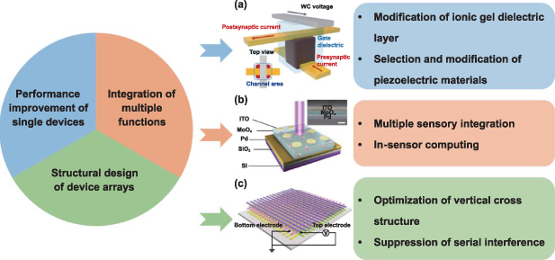
These issues can be solved by the following aspects (figure 12). (i) Performance improvement of single devices. By using a high dielectric constant ion gel as the gate dielectric layer, the EDL effect helps to reduce the operating voltage of the device and improve the modulation on charge carriers in the semiconductor channel. The flexibility, transparency, and biocompatibility of ion gel are also beneficial to neuromorphic devices [90]. In addition, expanding the selection of piezoelectric materials or modifying the pristine materials can also improve the device performance. Although SGTs are usually prepared with 1D wurtzite materials such as ZnO and GaN, the piezoelectric properties in 2D and bulk materials have also attracted much attention in recent years [22, 91–94]. Due to strain-induced lattice distortion and associated charge polarization, transition metal dichalcogenides exhibit large in-plane piezoelectricity, which can contribute to the construction of flexible and ultrathin piezotronic neuromorphic devices. Optimizing the semiconductor properties of 2D materials or exploiting the piezoelectricity of the substrate material can also enhance the output performance of the device [95, 96]. (ii) Integration of multiple functions. The first strategy is the construction of neuromorphic devices with multiple sensory integration. The piezoelectric effect naturally converts stress or strain signals into electrical signals to achieve bionic tactile perception. Furthermore, it is possible to use data fusion [97] or the inherent properties of functional materials to achieve multisensory sensing capabilities, such as using the optoelectronic effect for visual sensing [98]. Another strategy is to achieve the integration of sensing, storage, and computing functions. In-sensor computing can improve data processing capabilities and reduce or eliminate data transmission and device conversion [99]. (iii) Structural design of the device arrays. First, the remote gate controllability of dielectrics such as ion gel is exploited to improve the traditional two-terminal array of memristors to a three-terminal array of vertical gate-all-around FET structures, which can facilitate the exploitation of high performance and high density artificial neural networks as well as the applicability to smaller process junctions [100, 101]. In addition, there are many issues that remain to be addressed in building artificial neural networks, including decoupling of multiple sensor signals, crosstalk elimination, and on-chip integration [102].
Figure 12. Challenges and perspectives of piezotronic neuromorphic devices. (a) Performance improvement of single devices. Reproduced from [100]. CC BY 4.0. (b) Integration of multiple functions. Reproduced from [98], with permission from Springer Nature. (c) Structural design of device arrays. Reproduced from [101]. CC BY 4.0.
Download figure:
Standard image High-resolution image
In summary, piezotronic neuromorphic devices/systems are capable of sensing, computing, learning, and processing complex and specific problems, which is believed to be highly promising to facilitate the development of the Internet of Things, AI, biomedical engineering, and other fields.
Acknowledgments
This work is financially supported by the National Natural Science Foundation of China (52073031, 22008151), the National Key Research and Development Program of China (2021YFB3200304), Beijing Nova Program (Z211100002121148), Fundamental Research Funds for the Central Universities (E0EG6801X2), and the 'Hundred Talents Program' of the Chinese Academy of Sciences.