
Abstract
Holey Graphene (HG) is a widely used graphene material for the synthesis of high-purity and highly crystalline materials. The electronic properties of a periodic distribution of lattice holes are explored here, demonstrating the emergence of flat bands. It is established that such flat bands arise as a consequence of an induced sublattice site imbalance, i.e. by having more sites in one of the graphene's bipartite sublattice than in the other. This is equivalent to the breaking of a path-exchange symmetry. By further breaking the inversion symmetry, gaps and a nonzero Berry curvature are induced, leading to topological bands. In particular, the folding of the Dirac cones from the hexagonal Brillouin zone (BZ) to the holey superlattice rectangular BZ of HG, with sizes proportional to an integer n times the graphene's lattice parameter, leads to a periodicity in the gap formation such that  (mod 3). A low-energy hamiltonian for the three central bands is also obtained revealing that the system behaves as an effective
  graphene material. Therefore, a simple protocol is presented here that allows for obtaining flat bands at will. Such bands are known to increase electron-electron correlation effects. Therefore, the present work provides an alternative system that is much easier to build than twisted systems, allowing for the production of flat bands and potentially highly correlated quantum phases.
Export citation and abstract BibTeX RIS

Original content from this work may be used under the terms of the Creative Commons Attribution 4.0 license. Any further distribution of this work must maintain attribution to the author(s) and the title of the work, journal citation and DOI.
1. Introduction
In recent years, the concept of electronic flat bands has gained prominence in the fields of materials science and condensed matter physics [1–10]. This heightened interest can be attributed to the electronic, geometrical and topological properties inherent to flat bands [10–13] and their potential to give rise to novel phenomena [7, 14–20]. Specifically, the discovery of superconductivity in twisted bilayer graphene in 2018 fueled considerable attention in the field [7]. However, the primary challenge lies in the experimental control of the rotation angle. For this reason, alternative systems are currently being explored to preserve flat bands without relying solely on the rotation angle. Examples of these systems include graphene subjected to mechanical deformations [21–29] , multilayer graphene twisted (MTLG) under pressure [30–34], cyclicgraphyne, cyclicgraphdiyne [35] and holey graphene (HG) [36–39], where the theoretical possibility of chiral superconductivity emergence has been demonstrated [40].
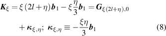
HG, also called graphene nanomesh, refers to the presence of holes distributed in the material [37, 41–43]. Introducing holes in graphene provides an additional degree of freedom to control optoelectronic and mechanical properties [44–46]. For example, holes create a mobility gap in graphene making it a narrow gap semiconductor [44]. This opens opportunities for exploring electronic, optical and correlated dependent phenomena and designing graphene-based devices that can exploit the unique properties of HG [42, 47–50]. Furthermore, the size and distribution of the holes can also modify the electronic properties. Using DFT calculations, Barkov and Glukhova [51] investigated HGs charge transmission in periodic arrays of holes.
Several techniques are employed to fabricate HG, including electron/ion beam lithography [47, 48, 52], plasma etching [47, 48], chemical etching [37], laser-based methods [53–58], and others [42, 43, 47–49, 59–63] . These techniques offer an experimental advantage over MTLG. Among them, the most common techniques used to fabricate HG are:
- Top-down lithography involves the selective removal of graphene sheets to create nanopores with uniform sizes and spatial arrangement. Although successful in producing graphene sheets with uniform nano-size pores, this technique faces challenges in large-scale fabrication and requires specialized equipment and expertise, making it expensive [47, 48, 52].
- Template-assisted chemical vapor deposition [42, 48, 52, 61]. In this method, HG is grown on specific inorganic templates. This technique allows for the bottom-up growth of HG and offers control over nanopores' size, shape, and distribution [61]. However, these fabrication techniques have certain drawbacks because they require careful control of various parameters such as temperature, pressure, and duration, making the process lengthy, cumbersome, and costly.
- Block copolymer lithography techniques on CVD-grown graphene [59, 64]. This technique involves patterning the graphene with a copolymer material and using reactive ion etching to create nanopores in the desired arrangement. One advantage of this technique is that it allows for the control of the neck width, which can be important in determining the properties and applications of HG. However, this approach still requires further optimization to achieve large-scale production of HG.
Nevertheless, laser-based methods have recently emerged as a promising technique for synthesizing HG [53–58]. These methods offer a precise means of controlling the synthesis process of the holey structure. Researchers can adjust parameters like laser intensity and target material to create holes with specific sizes, shapes, and distributions. This level of control enables the production of HG with tailored properties for various applications. Moreover, this method allows for the fabrication of high-purity and highly crystalline HG without the need for catalysts or chemicals. Laser ablation methods are also scalable, making them ideal for large-scale HG production. Furthermore, these techniques permit the customization of HG by introducing dopants and functional groups. This versatility contributes to the development of graphene-based devices with enhanced performance. However, it is worth noting some notable disadvantages, including the cost and complexity of the equipment, limited scalability for large-area synthesis of pristine graphene, and challenges in achieving structural uniformity.
In this work, we explore different configurations of HG which we show are able to produce flat-bands. From there, we study its electronic properties. The structure of this work is as follows: in section 2, we present the tight-binding model and the unit cells of the HG primarily under discussion. In section 3 we present the electronic properties of the systems introduced in section 2. Therein, the emergence of flat bands and energy gaps is discussed in terms of the Brillouin zone (BZ) folding and bipartite sublattices site imbalance. In section 4 we study the topological properties and present an effective low-energy model. Finally, our conclusions and future perspectives are outlined in section 5.
2. Tight-binding HG model
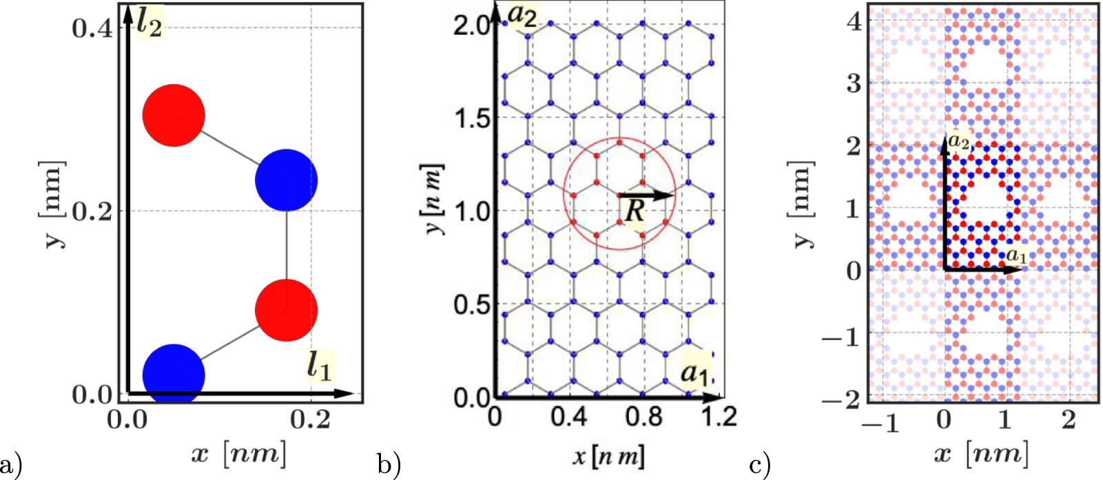
Our model is based on periodically distributed holes within a graphene lattice, maintaining translational symmetry. This enables us to simplify the treatment by leveraging Bloch's theorem. As seen in figure 1(a), we use a 4-atom superlattice unit cell containing the usual graphene non-equivalent sites A and B, where A and B refer to carbon atoms on each of the graphene's bipartite lattices, distinguished in the figure by colors blue and red, respectively.

Figure 1. a) Unit cell of graphene with a 4-atom basis and lattice vectors  arranged such that the zigzag and armchair directions align with the horizontal and vertical axes, respectively. (b) The unit cell used to build HG, featuring lattice vectors
  and
and  , where
  . Additionally, the atoms to be removed are highlighted in red, situated within a red circle of radius R. For notation purposes, we will designate this unit cell as UCHG
 . (c) Two-dimensional HG. Except in the case of (b), sites A are denoted in blue, while sites B are represented in red.
Download figure:
Standard image High-resolution imageAdditionally, we use two orthogonal lattice vectors:  and
and  , where
  Å is the carbon-carbon distance. As visually depicted in figures 1(a) and (b), this specific configuration ensures the alignment of the horizontal axis with the zigzag orientation and the perpendicular axis with the armchair orientation. We define the unit cell by employing lattice vectors
  and
and  (as shown in figure 1(b), where
  to ensure periodicity in the x direction, and similarly,
  is employed to establish periodicity in the y direction.
After obtaining the graphene lattice, we selectively remove atoms located within circles of radius R (Å) (refer to figure 1(c). It is worth noting that, without loss of generality, the circle delineating the atoms for removal is centered at  in the unit cell. As depicted in figure 1, we obtain a lattice featuring holes. We will denote the unit cell of graphene with a hole of radius R and vectors
  as UCHG
 .
.
Under such considerations, our investigation is based on a tight-binding model with only first-neighbors hopping transfer integral, which yields a Hamiltonian given by
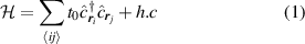
where  represents the sum over the neighbors with positions
r
i
and
r
j
that satisfy
represents the sum over the neighbors with positions
r
i
and
r
j
that satisfy  ;
;  is the creation (annhilation) operator and
  eV is the hopping integral between the ith and jth sites. Additionally, we numerically construct the Hamiltonian operator in reciprocal space
k
, which depends on the number of atoms in the unit cell and is denoted as
eV is the hopping integral between the ith and jth sites. Additionally, we numerically construct the Hamiltonian operator in reciprocal space
k
, which depends on the number of atoms in the unit cell and is denoted as  . The eigenvalues and eigenfunctions were thus numerically found by using Python dedicated libraries [65–67]. In the following section we will discuss the resulting electronic properties.
3. Electronic properties of bidimensional HG
This section is divided in three subsections, the first is devoted to present the band structure, the second analyzes the mechanism for flat band formation and the third explains the observed periodicity of gap formation.
3.1. Band structure and localization properties
In this section, we will discuss the electronic properties of systems with unit cells of type UCHG , focusing primarily on those depicted in figure 2, namely, UCH
 , UCHG
 , UCHG
 , UCHG
 , UCHG
 , and UCHG
 . These examples were chosen to include the effects of different radius and edge terminations. Observe that among our examples, in figure 2(f) we include the case of a hole with many sites of coordination one, akin to have dangling bonds, that will allow to discuss the origin of flat bands.

Figure 2. Six unit cells are displayed in which we vary the radius and the size of the corresponding lattice vectors for (a) UCHG , (b) UCHG
 , (c) UCHG
 , (d) UCHG
 , (e) UCHG
 , and (f) UCHG
 . This last case can be considered as the scenario for UCHG
 with the addition of six extra atoms with C3 symmetry, and it corresponds to a case of having sites with coordination one. The carbon atom colors indicate sites on each of the bipartite sublattices A and B.
Download figure:
Standard image High-resolution imageIn figure 3 we illustrate the bands obtained for each of the systems shown in figure 2. The BZ and high symmetry points are detailed in figure 4(c). As we can see, gaps are observed in some cases, while Dirac cones are seen in others. The opening of these gaps will be discussed later on in this section. More important for our purpose is that flat bands appear at energy E = 0, corresponding to the Fermi energy ( eV) at half-filling. Additional plots are provided in the

Figure 3. The band structure for systems with unit cells of (a) UCHG , (b) UCHG
 , (c) UCHG
 , (d) UCHG
 , (e) UCHG
 , and (f) UCHG
 are shown. It is observed that flat bands states exhibit a different IPR. Furthermore, for cases (a) to (d), it is noted that as n increases while maintaining R, the localization decreases; however, this does not hold true for case (f). This behavior can be understood in connection with the inbalance density
  , as discussed in the text. On the other hand, a consequence of maintaining dangling bonds distributed with C3 symmetry is the creation of a gap. This gap remains strongly protected even when increasing the size of the cell.
Download figure:
Standard image High-resolution image
Figure 4. Panels (a)–(b), spatial contribution to the Local Density of States (LDOS) for the UCHG and UCHG
 cells at E = 0, for the states corresponding to the flat band being associated with edge CLS on the zigzag boundaries of the holes. (c) The hexagonal Brillouin zone (BZ) of graphene is folded into the rectangular BZ of the HG. (d)–(e) Contribution of sublattice states in the band structure of UCHG
 , with the flat band resulting from the imbalance number through the path exchange symmetry [10, 74]. (f)–(g) The density of states,
  , is presented for the unit cells (f) UCHG(
 ) (black line), UCHG(
 ) (blue line), UCHG(
 ) (orange line), (g) UCHG(
 ) (black line), and UCHG(
 ) (red line). It is observed that
  decreases proportionally to the size of the cell n, as a consequence of the imbalance density
  as established in table 1.
Download figure:
Standard image High-resolution image
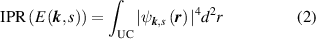
where  represents the wave function in the sth band, characterized by wave vector k and energy
  . Due to the periodic conditions of the lattice, the integral that appears in equation (2) is performed over the unit cell (UC). The IPR of an extended state goes as
  where N is the number of sites, while for localized states does not depend on N. For exponentially localized states, it can be proved that
  where λ is the localization length.
In figure 3, the  values for each
  are projected onto the band structure using a color code. In the
  . Such value is in perfect agreement with the numerical results seen in figure 3(a) for non-flat bands. Flat-bands in figure 3(a) have
  . How we interpret this value? First we remark here that the system is periodic even if holes are present, thus all states are in principle extended and will scale as
  , but with a slightly different participation. Secondly, we observe that flat band states preferentially spatially localize in the zig-zag boundary regions that form around the hole, as can be observed in figures 4(a) and (b). This allows to estimate the
  as follows. The number of sites in the hole edge seen in figure 3(a) is
  , from where the fraction
  . Taken this number as the fraction of active sites, we estimate that
  in reasonable agreement with the numerically observed value. The difference from the numerical value arises due to the fact that not only the sites at the hole's edge contribute; there are also sites close to the edge that contribute. In spite of this, the message here is that the flat-bands IPR shows a tendency for a decrease in their spatial participation when compared with others.
It is worth noting that these flat-band states are not the sole examples of increased IPR; in addition, we find quasi-flat bands within specific regions of the BZ that show a similar behavior, notably those with energies at  and momenta between the X and M points. Such behavior is due to the presence of Van Hove singularities in which a dimerization effect is seen [8, 29, 75].
To further confirm the nature of the states, in figures 4(a) and (b), we present the site contribution of the local density of states (DOS) for a flat band state in two different examples. It can be seen therein that participation in the flat band mainly occurs at the edges of the holes. From figures 3(a)–(d) and 4(a) and (b), it is observed that if n increases while R remains constant, or vice versa, the participation in the flat band decreases. However, for n = 9 and r = 5 such rule does not to hold since in addition, a gap opens.
3.2. Flat band formation mechanism: sublattice imbalance number and broken path-exchange symmetry
To gain a better understanding on the formation of flat bands, we introduce two parameters. The first one is the imbalance number, denoted as  and defined by,

which indicates the difference between number of sites A and B in the unit cell UCHG . The second is the imbalance density,
  ,
,

where N is the total number of atoms in each unit cell. The reason to define such quantities is that sublattice site imbalance in bipartite lattices is known to induce flat bands of confined states in other systems [76]. Such confinement is due to destructive interference [10]. Bipartite sublattice site imbalance can only occur in our periodic HG at hole edges. To see if such effect is in play , in table 1 we present the values for the site imbalance number, the site imbalance density, the energy gap, the DOS at E = 0 and the observed number of flat bands. Notice that in the last row of table 1 we included a case in which the imbalance number was made big by performing a tailor-made cut that maximizes the number of atoms in one sublattice along the hole rim. As seen in figure 2(f), this is equivalent to have dangling bonds or sites with coordination one in the rim.
Table 1. table displaying the number of imbalances,  , the imbalance density,
  , gap size, Δ, state density,
  , and the number of flat bands for graphene with a gap of size R [Å] and unit cells UCHG
 . Notice that in the last row, the imbalance number is big as the cut was chosen to increase the number of atoms in one sublattice along the hole rim. This is equivalent to have dangling bonds or sites with coordination one as seen in figure 2(f).
| n | R[Å] |

|

| Δ [eV] |

| No. Flat Bands |
|---|---|---|---|---|---|---|
| 5 | 3 | 1 |

|

|

| 1 |
| 7 | 3 | 1 |

|

|

| 1 |
| 9 | 3 | 1 |

|

|

| 1 |
| 7 | 5.2 | 1 |

|

|

| 1 |
| 9 | 5.2 | 1 |

|

|

| 1 |
| 9 | 5 | 7 |

|

|

| 7 |
From table 1 we observe that the number of flat bands perfectly matches the imbalance number for all the studied cases. Noteworthily, the last row of table 1, which contains the tailor-made site imbalance, produces the same number of flat bands. Therefore, we conclude that flat bands are produced by the sublattice imbalance and thus we can generate flat bands at will. Moreover, it has been demonstrated that flat bands appear as a consequence of brakening the path-exchange symmetry [10, 74]. Upon breaking, this symmetry introduces a complex phase [10, 74], leading to the lifting of the degeneracy while simultaneously preserving the flatness of the band. In the periodic holey system presented here, it can be demonstrated that the imbalance number is related to the path-exchange symmetry, and consequently the number of flat bands is equal to the imbalance number. The broken path-exchange symmetry distinguishes the sublattice with the highest number of sites. This is illustrated in figure 4, panels (d) and (e), for the case of HG , where the nonzero energy bands result from equal contributions from sublattices A and B.
Additionally, it is worth noting that the DOS or  , at E = 0 is directly proportional to the imbalance density (see table 1). In cases with no dangling bonds, we observe that
  , while
  (see figures 4(f) and (g)) for the lattice with dangling bonds. This can be understood by considering
  , where
  is the number of sites supporting the state with E = 0. Therefore,
  . In the studied cases without dangling bonds,
  fluctuates between
  sites (see for example figures 4(a) and (b)), and
  , maintaining an average ratio of 10.5 (see table 1 and figures 4(f) and (g)). For cases with dangling bonds, the states at E = 0 are strongly localized on sites with coordination one. Then
  corresponds to such number of sites and hence
  .
.
3.3. Gap formation mechanism: periodicity of the BZ folding
Let us know discuss the origin of the gaps. In figure 5 we present the gap size (Δ) evolution for three distinct graphene series with hole radii of  Å, in which the standard error of the gap,
  , and the standard error of the imbalance density,
  , for the three data series shown are
  eV and
  , respectively. Also, for each of these series, the size of the unit cell n is varied within the range
  , with the exception of the first series where
  . The initial observation in figure 5 is that for the series featuring hole radii of R = 3 and R = 5.2 Å, a periodicity with the property
  emerges for n sufficiently large, relative to the specific R value at which the gap reaches zero. This phenomenon is particularly evident in figures 3(c) and (e) where the emergence of Dirac cones at the Γ points is clearly observed.

Figure 5. Gap evolution as a function of n for different hole radius. Panel (a) is for R = 3 and panel (b) R = 5.2, both corresponding to systems without dangling bonds. Panel (c) corresponds to R = 5.0 which contains dangling bonds. The standard error of the gap,  , and the standard error of the imbalance density,
  , for the three data series shown are
  eV and
  , respectively. In cases (a) and (b), gapless systems occur with periodicity of
  . Otherwise, gaps are given by power law envelops in the form of
  . The following fittings laws were obtained, (a)
 . (b)
. (b)  and (c)
  where
where  is the statistical coefficient of determination.
Download figure:
Standard image High-resolution imageThe second observation that comes out from figure 5 is that excluding the semimetallic cases, Δ follows a power law for all cases,

where p is approximately 0.5166, 0.5797, and 0.6360 for the respective series and their statistical coefficient of determination  are 0.9997, 0.9947, and 0.9997.
In a previous work [44], it was found analytically and numerically that for graphene with random sustituitional disorder  . The nearly similar exponents indicate that in the end, big holes enter as nearly effective impurities. There are two reasons for this coincidence. The first is that impurities in the split band limit act as holes in the host lattice bands as wave functions are not able to penetrate such energy barriers [77]. The hole array acts as a third sublattice which produces the flat band as explained in section 4. It is akin to graphene with strongly biased circular patches [78]. The second reason for the square root scaling of the gap is that the chiral, electron–hole symmetric Hamiltonian when squared, removes one bipartite sublattice. Then E = 0 is the ground state of a triangular lattice with some underlying frustration [44, 76]. Sublattice imbalance leads to a perturbation on the Dirac cone mechanism of frustration in the triangular lattice [44]. Here the system is periodically perturbed and with some effective self-energy. This mechanism works in many other chiral systems [69].
However, Δ also oscillates. This is due to the periodic hole array perturbation perturbation and its relation with the unit cell size and geometry. In particular, now we will demonstrate that the gap periodicity arises due to the folding of the pristine graphene's BZ into the holey superlattice rectangular BZ (see figure 4(c)). To do this, consider the original Dirac points on each of the graphene's valley,
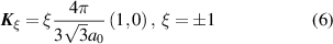
in the hexagonal BZ of graphene and ξ is the valley pseudospin index. On the other hand, consider the reciprocal vectors,
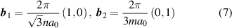
of HG with UCHG . It can be demonstrated that if
  with
with  and
and  , the following equation is obtained,
where
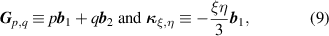
and therefore,  folds onto the point
  . In other words,
  folds along the path
  with a destination point determined by the η index and a period
  . Figure 6) presents, from n = 1 to n = 6, the folding sequence that results from equation (8). Notice that this result is independent of the size index m or hole radii R.

Figure 6. Brillouin zone of graphene and holey graphene with unit cell UCHG with
with  . The
. The  points are shown to be folded into
  for
for  and
and  (mod 3) (see equation (8)). In particular, for
  (mod 3), the
  folds to the Γ point, representing a valley degeneracy.
Download figure:
Standard image High-resolution imageIt is noteworthy that when η = 0,  folds to the Γ point, leading to valley degeneracy. Upon introducing holes in graphene (without dangling bonds), sublattice and inversion symmetries are broken, resulting in gaps at the Dirac points for
  [79–84]. However, Γ is a point protected by other symmetries, ensuring the preservation of the two degenerate cones when η = 0. To induce a gap at Γ, dangling bonds are necessary to break the path-exchange bond symmetry [85, 86]. Therefore, the imbalance density and the folding of the BZ explain the behavior of Δ seen in figure 5.
4. Topological properties and low-energy effective model
As is well known, flat bands in Moire systems are often topological. Thus it is interesting to explore the flat band topology of our HG system, and if possible, to build an effective low-energy model. Figure 7 shows the Berry curvature for the unit cells shown in figure 2 as a function of
k
and the band s. The Berry curvature is denoted as  and defined as,
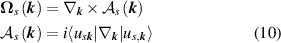
where  is the Berry connection and
  are the periodic functions in the Bloch states that solve the Schrödinger equation. Figure 7 illustrates how in some cases the symmetry breaking induces a nonzero Berry curvature at the folding points
  and in the vicinity of E = 0. However, in figures 7(c) and (e) we see that although the Dirac cones are preserved, the bands are non topological. This is due to the protection at the Γ point. Therefore, to have topological bands, it is necessary that n must not be divisible by three. Another option is to add dangling bonds. In summary, the flat bands discovered in this system are generally non topological, and are thus different from the moiré flat bands, which are often topological.

Figure 7. Color contour plot of the Berry curvature  as obtained from equation (10) for each band in the first Brillouin zone and along the indicated path. Panels correspond to exactly the same systems described on each panel of figure 3. In some cases, the broken symmetries induce a nonzero Berry curvature at the folding points
  and in the vicinity of E = 0. In panels (c) and (e), the Dirac cones are preserved but the bands are non topological. This is due to the protection at the Γ point. To have topological bands, it is necessary that n must not be divisible by 3.
Download figure:
Standard image High-resolution imageAs the electronic, optical and topological properties are determined mainly by electrons at the Fermi level, it is very convenient to develop a low-energy model to the system, akin to the Dirac effective equation that occurs in graphene. We start by observing that without dangling bonds and near the high-symmetry points  of the folded reciprocal lattice, three symmetric bands around E = 0 are formed, one for valence, the flat band, and the conduction band, denoted by
  , respectively. In other words, holes can be considered as a third sublattice producing an extra band. Folding the Dirac points at
  would, in principle, yield two bands with linear dispersion and a flat band at E = 0. Therefore, an appropriate Hamiltonian for this description is the
  model [87], defined by

where  with
with  a parameter, and
  , and
, and  are the pseudospin operators and Fermi velocity, respectively; given by
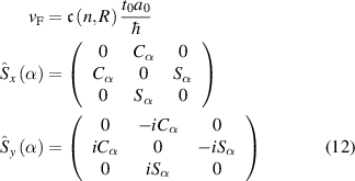
with  ,
,  and
and  a constant that depends on unit cell size n and hole size R. Such hamiltonian is the most simple one that has flat bands and under electromagnetic radiation, behaves as a two- or three-level Rabi system with clear optical signatures of flat bands [87].
As discussed previously, breaking inversion and sublattice symmetry results in the opening of a gap. Therefore, the low-energy Hamiltonian around  will exhibit an additional mass-like term to the
  Hamiltonian, thus the low-energy hamiltonian is

where  is a pseudospin operator defined as
and  is the mass-like term that depends on
k
and pseudospin index
is the mass-like term that depends on
k
and pseudospin index  . It can be constructed from the expansion of energies for the bands s, given by
where  can be numerically determined. Then
  is expressed as,

In figure 8, the electronic bands obtained from the Hamiltonian  (dashed black, blue and red lines) and the low-energy approximation with the Hamiltonian
  (equation (13)) (solid black, blue and red lines) are depicted. In general, an excellent agreement is obtained between the numerical and the low-energy effective model.

Figure 8. The electronic bands obtained from the Hamiltonian  (dashed black, blue, and red lines) are compared with the low-energy approximation using the Hamiltonian
  (solid black, blue, and red lines) for (a) UCHG
 ,
,  ,
,  eV,
eV,  eV nm, (b) UCHG
 ,
,  ,
,  eV,
eV,  eV nm, (c) UCHG
 ,
,  ,
,  eV,
eV,  eV nm, (d) UCHG
 ,
,  ,
,  eV,
eV,  eV nm and (f) UCHG
 ,
,  ,
,  eV,
eV,  eV nm. See equations (11)–(16). An excellent agreement between the low energy Hamiltonian and the tight-binding Hamiltonian is seen.
Download figure:
Standard image High-resolution image5. Concluding remarks
In this paper, we investigated the formation of flat bands in two-dimensional periodic HG (2D HG). Our findings reveal that these flat band states exhibit an increased IPR when compared to other states, particularly their have maximum density along the zigzag edges surrounding the hole. This highlights a connection between flat band formation and CLS, as investigated in prior works [10, 68, 69].
One of the main results established in this work is that flat bands arise as a consequence of an induced sublattice site imbalance, i.e. by having more sites in one of the graphene's bipartite sublattice than in the other. This is equivalent to break the path-exchange symmetry [10, 74]. Therefore, the results derived for the flat bands is completely general for bipartite sublattice site imbalance, but not in general for different folding schemes and hole shapes. Also, it was established that the breaking of both sublattice and inversion symmetries leads to the creation of energy gaps.
Furthermore, we have discussed the influence of unit cell size and hole dimensions on the gap size and DOS at E = 0, through the imbalance density  . Additionally, we have explored the existence of semimetallicity in 2D HG with a periodicity of
  , arising from the folding of
  points to the Γ point, protected by bond symmetry, except when introducing dangling bonds that break this symmetry, resulting in a gap. We demonstrated that the breaking of the discussed symmetries (inversion, sublattice, and bond) can generate a non-zero Berry curvature. However, in many cases the flat bands discovered here can also be non topological, and are thus different from the moire flat bands, which are often topological.
Finally, we establish a continuous Hamiltonian model for three bands in cases where the hole radius R ≠ 0 and there are no dangling bonds. This model consists of an  type Hamiltonian and a mass-like term that opens the gap at
  points.
Our work gives a protocol that allows to obtain flat bands at will and thus gives a possible new 2D material to obtain highly correlated quantum phases without twists.
Acknowledgments
This work was supported by CONAHCyT Project 1564464 and UNAM DGAPA Project IN101924. Abdiel de Jesús Espinosa-Champo is supported by a CONAHCyT PhD fellowship (No. CVU 1007044). The authors acknowledge and express gratitude to Carlos Ernesto López Natarén from Secretaria Técnica de Cómputo y Telecomunicaciones for helping with the high performance computing infrastructure at Instituto de Física, UNAM, where we run our calculations and his valuable support.
Data availability statement
All data that support the findings of this study are included within the article (and any supplementary files).
Appendix:
In this appendix we present the bands for bigger systems than those studied in the main text. Figure 9 presents three representative cases and its corresponding IPR. Flat bands are clearly seen as expected as site imbalance and not size determine its existence. To further confirm this point, in figure 10 we plot the contribution of each bipartite sublattice to the bands. The flat band is clearly sublattice polarized as expected form site imbalance.

Figure 9. The band structure for large systems with unit cells of (a) UCHG , (b) UCHG
 , and (c) UCHG
 are shown.
Download figure:
Standard image High-resolution image
Figure 10. Contribution of each bipartite sublattice to the band structure of (a)–(b) UCHG , (c)–(d) UCHG
 , (e)–(f) UCHG
 . Notice how the flat band is clearly sublattice polarized due to the imbalance number, i.e. broken path exchange symmetry [10, 74].
Download figure:
Standard image High-resolution image