
Abstract
The study of photovoltaic solar cells has been an exciting field of research because of their environmentally friendly nature. Scientists are continuously searching for new methods to develop solar cells that are highly efficient and cost-effective. One promising option is the use of Copper Antimony Sulphide (CuSbS2) based ternary compound semiconductor in ultrathin film photovoltaic cells. This material has a high absorption coefficient, low cost, and is readily available in the earth's crust. These characteristics make it an ideal candidate for use as a thin-film absorber layer in solar cells. In this work, FTO/CdS/In2S3/CuSbS2/Spiro-OMeTAD/Au device is proposed to improve the efficiency of experimentally designed CuSbS2-based thin film solar cells using numerical modeling. Device simulation was carried out using SCAPS-1D software, and the illumination spectrum used for this optimization was 1.5 AM. The simulated results from SCAPS-1D were compared to the experimental data. After optimizing the device parameters all the electrical parameters of the solar cell were improved. The optimized CuSbS2-based device shows power conversion efficiency (PCE) of 21.11% with short circuit current density (Jsc) of 20.96 mA cm−2, open circuit voltage (Voc) of 1.23 V, and fill factor (FF) of 81.84%. Based on the simulation results, it is possible to increase the performance of the device by varying different parameters such as the defect density of each layer, interfacial defect density, thickness, and doping concentration.
Export citation and abstract BibTeX RIS

Original content from this work may be used under the terms of the Creative Commons Attribution 4.0 licence. Any further distribution of this work must maintain attribution to the author(s) and the title of the work, journal citation and DOI.
1. Introduction
The growing energy requirements and the rapid depletion of non-renewable energy sources have led to a focus on finding alternative sources of energy. One such prominent source is the solar cell, which is a non-renewable energy source that has gained significant attention. The silicon-based solar cell was first introduced into the market and still, they are dominating in the solar cell market. For the manufacture and production of silicon-based solar cells, sophisticated fabrication procedures are needed, which drives up the cost of the solar panel [1]. A popular area of research in the photovoltaic industry is using of thin film technology which utilizes less material to fabricate solar cells by depositing semiconductor materials. Thus thin film technology is more affordable than other technologies. As production capacities advance, thin-film solar cells are growing in popularity [2].
As photovoltaic absorbers, a variety of bulk and thin-film materials are being investigated [3–15]. Laboratory scale power conversion efficiency of 23.3% and 22.1% were attained for Cu(In, Ga)(S, Se)2 and CdTe thin film solar cells [16]. However, the long-term utilization and sustainability of the In, Ga, and Cd elements are problematic due to their scarcity and toxicity [17]. Cu2ZnSnS4 (CZTS) is an effective material for absorbing solar energy and can be used as a photocatalyst. CZTS can replace commonly used materials such as CIGS and CdTe, and it is considered a suitable alternative due to its low cost and the fact that it is made from easily obtainable elements, such as zinc and tin, rather than more expensive indium [18]. Additionally, CZTS is a safe material, and its production does not rely on rare or hazardous materials [19]. The most efficient CZTS (copper zinc tin sulfide) thin film solar cells have been achieved through vacuum techniques, with a maximum efficiency of 10%. However, there are several challenges associated with CZTS solar cells, including the need to ensure the formation of single-phase crystalline films, precise control of the composition of the elements, and preventing the formation of unwanted binary and ternary secondary phases such as Cu2S, SnS2, Sn2S3, Cu2SnS3, Cu3SnS4, and Cu4SnS4 [20]. In addition to CZTS and CdTe thin-film solar cells, Antimony selenide (Sb2Se3) is a relatively new member of the thin-film photovoltaic family and is considered to be some of the best potential absorber material options available among inorganic semiconductors. Its features include an optical bandgap of 1.2 eV, a high absorption coefficient of >105 cm−1, moderate carrier mobility of 10 cm2/Volt-Second, extended carrier lifetime of 60 ns, and low cost in addition to being harmless and earth-abundant [21]. However, there are some challenges associated with Sb2Se3-based thin film solar cells. These include stability, toxicity of Antimony, and fabrication complexity. To overcome all these problems, research has been focused on CuSbS2-based solar cells due to their favorable physical and chemical properties as a means of addressing the challenges faced by current solar cell technology.
Copper antimony sulphide (CuSbS2), a ternary semiconductor material, is a potential absorber material that can be used for photovoltaics applications. CuSbS2 gains researchers attention due to its low cost, non-toxicity, high absorption coefficient, and earth-abundant [22–26]. It has attractive optical characteristics, such as inherent p-type conductivity [27] and bandgap from 1.08–1.45 eV [28, 29]. Furthermore, a variety of techniques, including thermal evaporation [30–33], sputtering [34, 35], solution processing [36], spin coating [15], electrodeposition [32, 37], spray pyrolysis [38–40] and chemical bath [41–43] can be used to deposit CuSbS2.Thus, CuSbS2 is a potential absorber for inexpensive and highly efficient solar cells.
Despite several studies emphasizing the potential of CuSbS2 thin films as absorbers and focusing on their optical, electrical, and structural characteristics, only a small number of studies have shown how useful CuSbS2 is in actual solar systems [44]. The first CuSbS2 based solar cells with a Voc of 345 mV and a very low Jsc of 0.2 mA cm−2 were published in 2005 [45] using the chemical bath deposition procedure. Various techniques can be used to fabricate CuSbS2 based solar cells. The PCE of all of the CuSbS2 based solar cells that have been developed so far is usually below 2% [46–49]. Using a hybrid ink method, Banu et al developed CuSbS2 based solar cells in 2016 and obtained the greatest PCE of 3.22% with a Voc of 470 mV [2]. It is understood that the absorber layer flaws and dominant interfacial recombination of minority carriers limit the performance of CuSbS2 solar cells [50–52].
In this study, a solar cell capacitance simulator (SCAPS-1D) was used to analyze the structure of solar cell FTO/CdS/In2S3/CuSbS2/Spiro-OMeTAD/Au and it is compared with the experimental data [53]. Investigations have been done to know how the physical characteristics of absorber layer, buffer layer affect the PV performance of the newly developed solar cell. Even though similar types of works exist in literature, the novelty of this work is we have replicated the experimental results by numerical simulation and, we have studied how to improve device PCE with material properties. It is found that PCE of the device enhances from 1.86%-21.11% by varying the thickness, defect density of the absorber layer, acceptor concentration of absorber layer, interfacial defect density, and series resistance.
2. Device modeling and solar cell structure
This article discusses a study that involves a detailed investigation of the design proposed by Joel van Embden et al [53]. The investigation was conducted through simulation analysis, which utilized the SCAPS-1D tool [54]. Using this software we can use up to seven layers of semiconductors by using three basic equations i.e. Poisson equation, electron continuity equation, and hole continuity equation. With the aid of these three equations, we can estimate how well a solar cell will function in a variety of environments, including varying illumination conditions and semiconductor material doping levels [26, 55].
Here is the Poisson equation,

the continuity equation for electrons is,

and the continuity equation for holes is,

In equations (4) and (5), the drift-diffusion equations for charge carriers are presented, which are used to determine the current density of electrons and holes in a solar cell. It informs the movement of charged particles due to both the electric field (drift) and random thermal motion (diffusion) in the semiconductor material of the solar cell. By solving these equations, it is possible to calculate the flow of charge carriers


Here x is the coordinate position, φ denotes electrostatic potential, ε is relative permittivity, n is the concentration of electrons, p is the concentration of holes, q is the electron charge, ntr represents trapped electrons, and ptr represents trapped holes, respectively. Meanwhile, ND + is ionized donor doping concentration, NA - is ionized acceptor doping concentration, Jn denotes electron current density, Jp denotes hole current density, G is generation rate, Rn is electrons recombination rate, Rp is holes recombination rate, Dn is diffusion coefficient of electrons, Dp is diffusion coefficient of holes, μn is electron mobility, and μp is hole mobility, respectively.
The device structure FTO/CdS/In2S3/CuSbS2/Spiro-OMeTAD/Au with energy band diagram is shown in figure 1. Here, Au, Spiro-OMeTAD, and CuSbS2, were used as back contact, hole transport layer (HTL), and p-type absorber layer respectively. Both CdS and In2S3 act as n-type buffer layers whereas FTO acts as transparent conductive oxide. The parameters used in the simulation were taken from the literature [26, 55–59].
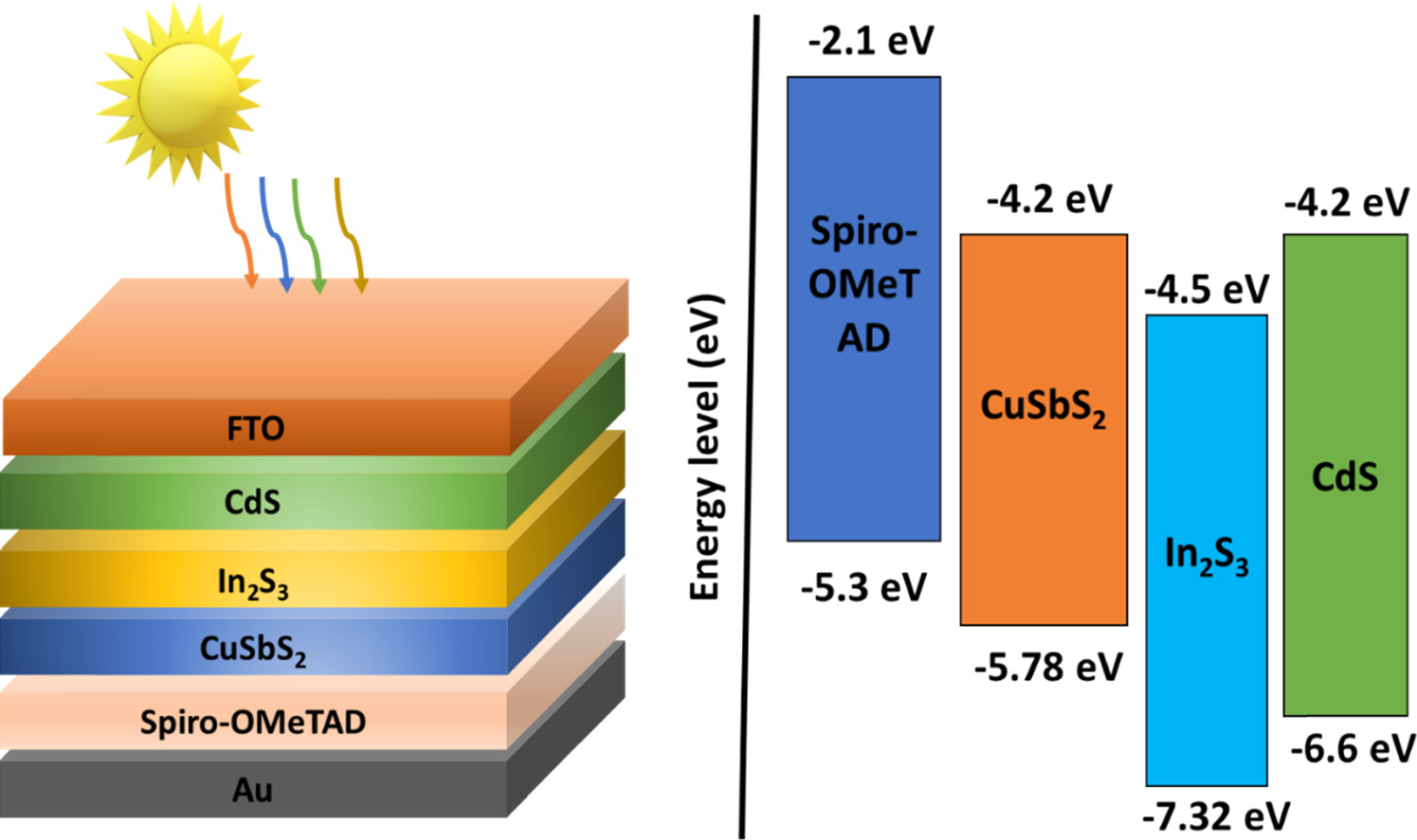
Figure 1. Device structure with energy band diagram.
Download figure:
Standard image High-resolution image3. Results and discussion
Simulations were first carried out to match the results with experimentally fabricated solar cells. After finding the parameters we then optimize the device parameters and how its performance can be improved is discussed in depth. We made every effort to perform our simulations using the same parameters as the experimental solar cells during comparison.
3.1. Experimental results validation
With the aid of simulation tool, we have verified the experimental findings that have already been published [53]. Figure 2(a) shows the SEM image of the solar cell architecture (Reprinted with permission from {56}. Copyright {2020} American Chemical Society). FTO (450 nm), CdS (90 nm), In2S3 (60 nm), CuSbS2 (180 nm), Spiro-OMeTAD (125 nm), and Au were the layers(thickness) used to fabricate the solar cells considered in the published work [53]. First, a layer of CdS was deposited onto FTO using Chemical bath deposition(CBD). Then a buffer layer of In2S3 was deposited. Next, the absorber layer CuSbS2 was deposited by spin-coating. Afterward, a hole transport layer made of Spiro-OMeTAD was deposited by spin coating. At last, Au electrodes were deposited through a photoresist by thermal evaporation. The first experimental solar cell results from [53] were replicated in SCAPS software for comparison and verification of our proposed approach. The J-V curves comparison of the experimental and simulated model is shown in figure 2(b), and it was interesting to see that the SCAPS software consistently produced outcomes that were similar to those obtained through experimental work. All the simulation parameters were shown in table 1. Thickness and bandgap of all layers were taken from experimental work [53]. Except acceptor density of the absorber layer, defect density of all layers, interfacial defect density, and series resistance of the device, remaining all simulation parameters and experimental validation parameters are the same. The simulated solar cell results are compared with experimental work and the details are given in table 2.

Figure 2. (a) SEM image of CuSbS2-based solar cell [Reprinted with permission from [44]. Copyright (2020) American Chemical Society.] (b) Comparison of experimental and simulated J-V curves before optimization.
Download figure:
Standard image High-resolution imageTable 1. Material Parameters Used In Device Numerical Modelling [26, 55–59].
| Parameters | Spiro-OMeTAD | CuSbS2 | In2S3 | CdS | FTO |
|---|---|---|---|---|---|
| Thickness (μm) | 0.125 | 0.18 | 0.06 | 0.09 | 0.45 |
| Band-gap (eV) | 3.2 | 1.58 | 2.82 | 2.4 | 3.2 |
| Electron affinity (eV) | 2.1 | 4.2 | 4.5 | 4.2 | 4.4 |
| Relative permittivity | 3 | 14.6 | 13.5 | 10 | 9 |
| Conduction band density of states (cm−3) | 2.5 × 10¹⁷ | 2 × 10¹⁷ | 2 × 10¹⁸ | 2.2 × 10¹⁸ | 2.2 × 10¹⁸ |
| Valence band density of states (cm−3) | 1.8 × 10²⁰ | 1 × 10²⁰ | 1.8 × 10¹⁹ | 1.8 × 10¹⁹ | 1.8 × 10¹⁹ |
| Thermal Velocity (cm/s) | 1 × 10⁷ | 1 × 10⁷ | 1 × 10⁷ | 1 × 10⁷ | 1 × 10⁷ |
| Electron mobility (cm2/vs) | 0.0002 | 49 | 100 | 100 | 20 |
| Hole mobility (cm2/vs) | 0.0002 | 49 | 25 | 25 | 10 |
| Donor Concentration, (cm−3) | 0 | 0 | 1× 10¹⁵ | 1 × 10¹⁷ | 1 × 10¹⁸ |
| Acceptor Concentration, (cm−3) | 1 × 10²⁰ | 1.38 × 10¹⁸ | 0 | 0 | 0 |
| Defect Density (cm−3) | 1 × 10¹⁴ | 1 × 10¹⁴ | 1 × 10¹⁴ | 1 × 10¹⁵ | 1 × 10¹⁵ |
Table 2. Comparison Of Experimental Solar Cell With Simulation Work (Considering the experimental data of thickness, bandgap, and other parameters).
| Method | VOC (V) | JSC (mA/cm2) | FF (%) | PCE (%) |
|---|---|---|---|---|
| Experimental | 0.48 | 6.45 | 55.2 | 1.72 |
| Simulation | 0.46 | 7.69 | 52.7 | 1.86 |
3.2. Effect of CuSbS2 absorber layer thickness on device performance recommendations
Absorber layer thickness plays a vital role in determining the efficiency of solar cells. When the diffusion length equals or exceeds the thickness of the absorber layer, rear contact recombination becomes the primary loss mechanism in the solar cell. When the absorber layer is very thin, efficiency and the absorption rate are less. Conversely, when the absorber layer is very thick, the charge carriers may not migrate up to the charge collecting layers [60]. Here, the absorber layer thickness was varied from 0.1 μm to 1.0 μm to investigate the effect of absorber layer thickness on the performance parameters of solar cells. Figure 3. shows the effect of thickness on Voc, Jsc, FF, and PCE. With the increase of absorber layer thickness from 0.1 μm to 1.0 μm, PCE increases from 8.37%- 21.11% and parameters like Voc, Jsc, FF also increases. This is because thicker absorber layers absorb more photons with higher wavelengths, resulting in more electron–hole pairs and an increased quantity of electron capture.
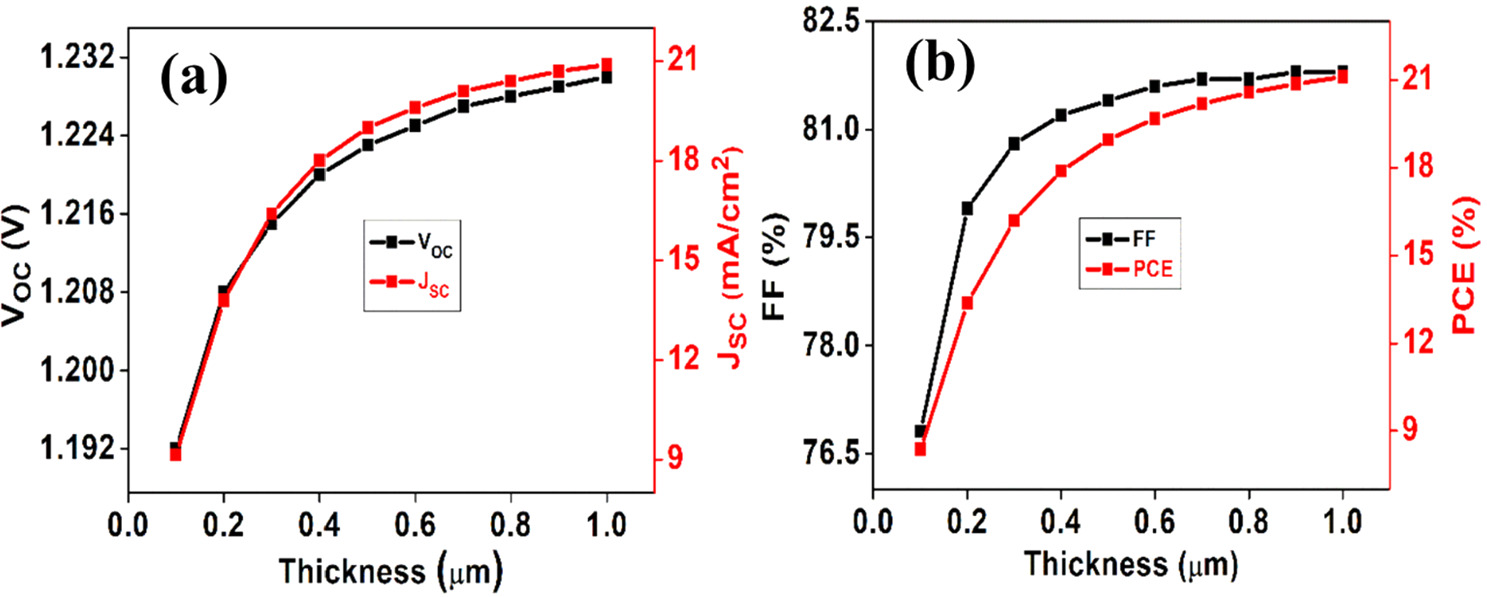
Figure 3. Effect of absorber layer thickness on Voc, Jsc, FF and PCE.
Download figure:
Standard image High-resolution imageAccording to equation (6), the Voc depends on both the Jsc and Jo, therefore it increased initially more quickly and then more slowly as the thickness of the absorber layers increased. The number of photo-generated carriers increases as the thickness of the absorber layer increases, leading to an initial rise in Voc.

Figure 4(a) shows the J-V curves of the simulated solar cell with different thicknesses of the CuSbS2 absorber layer. From the graph, large rise in Jsc is observed as the thickness of absorber increases. This is due to greater absorption that results in a greater number of electron hole pairs generation. Although electron–hole pairs are produced beyond a thickness of around 0.7 μm, the increase in Jsc is not significant because the electron and hole pairs must travel a greater distance for diffusion and then recombine before reaching the contact electrode. Quantum efficiency (QE) curves for different thicknesses of absorber layer are shown in figure 4(b). It is observed that better QE curve is obtained as the thickness increases. QE curves do not significantly increase after a particular optimal thickness when the thickness is further increased. There is a better QE curve at higher wavelengths at increased thickness because high-energy photons are absorbed on the front surface and low-energy photons require a thick enough absorber layer.

Figure 4. J-V and QE characteristic curves for various thickness of absorber layer.
Download figure:
Standard image High-resolution image3.3. Effect of CuSbS2 defect density on PV parameters of solar cell
Defect density has a significant impact on the performance parameters of the solar cell. In this simulation, the defect density of the absorber layer varied from 1014–1018 cm−3. Figure 5. shows the effect of the defect density of CuSbS2 on PV parameters of the solar cell. With the increase of defect density from 1014− 1018 cm−3, PCE decreases from 12.60% to 5.47%. From figures 5(a) and (b), it is observed that all PV parameters are influenced by defect density. This is due to the improvement in the recombination process, which results in the destruction of the charge carriers [61]. A low defect density results in a high charge carrier diffusion length and a low rate of recombination, which improves performance parameters.

Figure 5. Impact of absorber defect density on Voc, Jsc, FF and PCE.
Download figure:
Standard image High-resolution image3.4. Effect of operating temperature on device performance
The performance of thin film solar cell is significantly influenced by the operating temperature. Incident light causes heating on solar cells, which has an impact on PV cell performance. In this work, the operating temperature of the device was varied from 300-350 K. The simulation results of temperature versus Voc, Jsc, FF, and PCE are shown in figure 6. From figure 6(a) it is observed that Voc decreases and Jsc increases with increasing temperature. The reason for the increase in Jsc with the rising temperature is due to the drop of the bandgap energy of semiconductor materials which will involve in the generation of more electron–hole pairs. It can be found according to equation (7).

Where Jo is reverse saturation current, Je is light-induced photocurrent. According to equation (7), as temperature increases Jo increases and this rise in current is the primary factor causing the decrease in Voc. The energy of electrons increases with operating temperature. Due to high temperature, these electrons are much more probable to recombine with holes before they reach the depletion area.

Figure 6. Influence of temperature on solar cell parameters Voc, Jsc, FF, and PCE.
Download figure:
Standard image High-resolution image3.5. Energy band diagram of the proposed solar cell
In the FTO/CdS/In2S3/CuSbS2/Spiro-OMeTAD/Au solar cell, in figure 7. the energy band diagram illustrates how the different layers work together to generate electrical power from sunlight. The first layer in the solar cell is FTO, which acts as a transparent conductive oxide and forms the front electrode. The next layer is CdS a n-type buffer layer that is deposited on top of FTO. It has a lower conduction band edge than In2S3, creating a barrier for electrons to flow from In2S3 to FTO. In2S3 is also a n-type buffer layer that is deposited on top of CdS. It has a higher conduction band edge than CdS, creating a built-in potential that drives electrons to flow from In2S3 to CuSbS2. CuSbS2 is a p-type semiconductor and the absorber layer in the solar cell. It is sandwiched between the n-type In2S3 and Spiro-OMeTAD layers. The valence band edge of CuSbS2 is higher than the Fermi level of In2S3/Spiro-OMeTAD, creating a built-in potential that drives holes to flow from CuSbS2 to In2S3/Spiro-OMeTAD. Spiro-OMeTAD is the hole transport layer, which facilitates the movement of holes from CuSbS2 to the back electrode, which is typically a metal like Au. The valence band edge of Spiro-OMeTAD is higher than the Fermi level of Au, creating a built-in potential that drives holes to flow from Spiro-OMeTAD to Au. Au (Gold) is used as the back electrode and it completes the solar cell structure. The Fermi level of Au is higher than the valence band edge of Spiro-OMeTAD, creating a barrier for holes to flow from Au to Spiro-OMeTAD.

Figure 7. Energy band diagram of the solar cell.
Download figure:
Standard image High-resolution image
The efficiency of CuSbS2 solar cells is limited by the low Voc due to a disadvantageous conduction band offset (CBO) between CuSbS2 and CdS buffer layer. It is important to find a suitable buffer layer that can minimize this band misalignment. In2S3 is a direct band gap material with a band gap of 2.82 eV, making it transparent to the solar spectrum, and could potentially serve as an ideal buffer layer for CuSbS2 solar cells. Despite the misalignment between CuSbS2 and CdS buffer layer, In2S3 could help improve the efficiency of the cells.
4. Conclusion
We analyzed CuSbS2 thin film solar cells and further used simulation to verify the experimental findings reported by Joel van Embden et al in a similar device design. Using similar device materials, our simulation yields a PCE of 1.86% which is 8% higher than the experimentally achieved value of 1.72%. Different absorber layer parameters were varied to further improve the performance of the device. In order to make our work more realistic and workable, bulk and interfacial flaws have also been considered. With regard to device performance, our simulation work offers insights into defining Photovoltaic parameter limitations and comprehending their interdependency. Additionally, it aids in determining the optimal value for different device layer thicknesses, defect densities, and their relationship to device performance. In the FTO/CdS/In2S3/CuSbS2/Spiro-OMeTAD/Au configuration, the enhanced device showed an efficiency of around 12.60% for the absorber thickness of 0.18 μm which is higher than the previous study and for the absorber thickness of 1 μm we achieved PCE of 21.11%. With Jsc of 20.96 mA cm−2, Voc of 1.23 V, and FF of 81.84%, the enhanced design exhibited great device performance when defects were considered. However, the software has certain limitations when compared to the experimental side, particularly in the case of device stability testing, which necessitates a specific focus on improvisation from the software developer end. Even while the software is limited in its ability to account for all potential issues that may develop during experimental work, it can still serve as a clear roadmap for achieving such high performance practically in the coming years.
Acknowledgments
Naga Jyothi Valeti and Krishna Prakash acknowledge the SRM University AP for providing a University PhD and University Postdoctoral fellowship respectively.
Data availability statement
The data that support the findings of this study are available upon reasonable request from the authors.