Experimental Techniques ( IF 1.6 ) Pub Date : 2023-10-27 , DOI: 10.1007/s40799-023-00679-5 M.-K. Shih , Y.-H. Liu , G.-S. Lin , E. Hsu , J. Yang
|
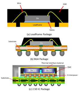
Microelectronics packages play a vital role in not only interconnecting the electronic signals from the die to the printed circuit board (PCB), but also in protecting the chips during the manufacturing process and their subsequent service lives. Epoxy molding compound (EMC) is widely used in electronic packaging due to its superior processing capability and low circuit signal delay. However, interfacial delamination is a common problem in encapsulated silicon devices, particularly at the interface between the copper leadframe (LF) pads and the EMC due to the weaker adhesion strength. Accordingly, the present study employs a double cantilever beam (DCB) experimental testing method and a numerical model based on the virtual crack closure technique (VCCT) to investigate the fracture behavior at the EMC/Cu LF interface in a quad flat no leads (QFN) package. The experiments are performed on an MTS-Acumen microforce tester equipped with a load unit capable of applying a force of 0.01 to 1250 N with a displacement resolution of 0.1 μm. The DCB specimens are prepared with a pre-crack length of 12 mm. The validity of the simulation model is confirmed by comparing the predicted values of the critical strain energy release rate (SERR, Gc) between the EMC and the copper LF pads with the experimental observations. In general, the results show that the Gc value provides a useful parameter for evaluating the delamination risk of encapsulated microelectronics packages and assessing the reliability of alternative package architectures.
中文翻译:
封装微电子封装中环氧模塑料 (EMC) 和金属之间分层的实验和数值研究
微电子封装不仅在将电子信号从芯片互连到印刷电路板 (PCB) 方面发挥着至关重要的作用,而且在制造过程及其后续使用寿命期间保护芯片方面也发挥着至关重要的作用。环氧模塑料(EMC)因其优越的处理能力和低电路信号延迟而广泛应用于电子封装。然而,界面分层是封装硅器件中的一个常见问题,特别是在铜引线框架 (LF) 焊盘和 EMC 之间的界面处,因为粘合强度较弱。因此,本研究采用双悬臂梁(DCB)实验测试方法和基于虚拟裂纹闭合技术(VCCT)的数值模型来研究四方扁平无引线(QFN)中EMC/Cu LF界面的断裂行为) 包裹。实验在配备负载单元的 MTS-Acumen 微力测试仪上进行,负载单元能够施加 0.01 至 1250 N 的力,位移分辨率为 0.1 μm。DCB 试样的预裂纹长度为 12 mm。通过将 EMC 和铜 LF 焊盘之间的临界应变能释放率 (SERR, G c )的预测值与实验观察结果进行比较,证实了仿真模型的有效性。总的来说,结果表明 G c值为评估封装微电子封装的分层风险和评估替代封装架构的可靠性提供了有用的参数。


 京公网安备 11010802027423号