Applied Physics B ( IF 2.1 ) Pub Date : 2024-01-10 , DOI: 10.1007/s00340-023-08164-y Jianan Xie , Tao Lin , Cailin Wang , Jiahao Shi , Chaoyang Xie , Duo Liang , Yupeng Duan
|
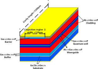
Since there are few research reports on semiconductor lasers in the yellow wavelength, this manuscript proposes the design of a semiconductor laser with an excitation wavelength of 589 nm, using a Ge/SiGe substrate, combined with GaInP quantum wells with high Ga composition and AlGaInP series of materials as the main structural layer of the laser. Simulation software is used for feasibility verification, and the effects of different parameters are discussed to optimize the device structure. The effects of interfacial states and electron leakage on the device characteristics are discussed, and a solution to the electron leakage problem is given. The results show that under the influence of the interfacial state, the threshold current of the 589-nm laser reaches 3.3 A, and the output power is about 0.6 W. Through optimization, by adding two layers of AlP electron-blocking layer with a thickness of 5 nm between the P-type cladding and the upper waveguide layer, the concentration of electrons in the P-type cladding layer can be reduced to 1.53 × 1015 cm−3, the threshold current of the device is reduced to 2.13 A, and the output power reaches 0.87 W.
中文翻译:
Ge/SiGe衬底上589nm GaInP量子阱半导体激光器的研究
由于黄光波长半导体激光器的研究报道较少,本文提出了一种激发波长为589 nm的半导体激光器的设计,采用Ge/SiGe衬底,结合高Ga成分的GaInP量子阱和AlGaInP系列材料作为激光器的主要结构层。利用仿真软件进行可行性验证,并讨论不同参数的影响,优化装置结构。讨论了界面态和电子泄漏对器件特性的影响,并给出了电子泄漏问题的解决方案。结果表明,在界面态的影响下,589 nm激光器的阈值电流达到3.3 A,输出功率约为0.6 W。通过优化,通过增加两层AlP电子阻挡层,厚度为P型包覆层与上波导层之间的厚度为5 nm,P型包覆层中的电子浓度可降低至1.53×10 15 cm -3,器件的阈值电流降低至2.13 A,输出功率达到0.87W。


 京公网安备 11010802027423号